Synchronous type semiconductor device
a semiconductor device and synchronous technology, applied in the field of synchronous semiconductor devices, can solve the problems of reducing the operating margin when operating at a high frequency, and achieve the effects of preventing erroneous information samples, stable operation, and reducing the pulse width of each internal clock signal
- Summary
- Abstract
- Description
- Claims
- Application Information
AI Technical Summary
Benefits of technology
Problems solved by technology
Method used
Image
Examples
first embodiment
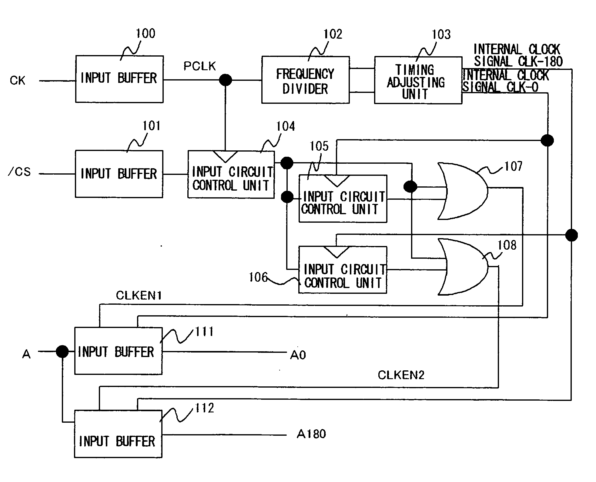
[0075]FIG. 3 is a diagram showing a configuration of a synchronous type semiconductor device according to the present invention, and corresponds to a configuration (an input portion of a synchronous DRAM) in FIG. 1. The input buffer 100, frequency divider 102, and timing adjusting unit 103 constitute a clock generation circuit. The timing adjusting unit 103 includes delay circuit or the like. The input buffer 100 receives the external clock signal CK. The frequency divider 102 frequency divides an output of the input buffer 100. The timing adjusting unit 103 receives an output of the frequency divider 102 and generates the two-phase internal clock signals CLK-0 and CLK-180.
[0076] The input buffer 101 receives the chip select signal / CS. The input buffer 101, input circuit control units 104, 105 and 106, and OR circuits 107 and 108 constitute a chip select circuit.
[0077] The input circuit control unit 104 latches and outputs the chip select signal output from the input buffer 101 res...
second embodiment
[0089] Next, another embodiment of the present invention will be described. FIG. 5 is a diagram showing an overall configuration of a synchronous type semiconductor device according to the present invention.
[0090] This embodiment includes the input buffer 100, frequency divider 102, timing adjusting unit 103, input buffer 101, input circuit control unit 109, input circuit control unit 110, input circuit control unit 105, input circuit control unit 106, OR circuit 107, and OR circuit 108. The input buffer 100 receives the external clock signal CK. The frequency divider 102 frequency divides the clock signal (PCLK) output from the input buffer 100, thereby outputting the first frequency-divided clock signal DIVCLK1 and the second frequency-divided clock signal DIVCLK2 having different phases. The timing adjusting unit 103 receives the first frequency-divided clock signal DIVCLK1 and the second frequency-divided clock signal DIVCLK2 from the frequency divider 102 and generates the two-...
PUM
 Abstract
Description
Claims
Application Information
 - R&D
- Intellectual Property
- Life Sciences
- Materials
- Tech Scout
- Unparalleled Data Quality
- Higher Quality Content
- 60% Fewer Hallucinations
Browse by: Latest US Patents, China's latest patents, Technical Efficacy Thesaurus, Application Domain, Technology Topic, Popular Technical Reports.
© 2025 PatSnap. All rights reserved.Legal|Privacy policy|Modern Slavery Act Transparency Statement|Sitemap|About US| Contact US: help@patsnap.com


