Semiconductor light source with optical feedback

a technology of semiconductors and light sources, applied in the field of semiconductor light sources, can solve the problems of spurious md photocurrent noise in the apc circuit, power control errors, and inability to compensate for the decline in brightness with device ag

Inactive Publication Date: 2007-03-22
USL TECH
View PDF19 Cites 18 Cited by
  • Summary
  • Abstract
  • Description
  • Claims
  • Application Information

AI Technical Summary

Benefits of technology

[0012] In another aspect of the invention, a groove is formed in the top horizontal surface to receive an edge of a beam splitter plate to assist in positioning the beam splitter plate.

Problems solved by technology

This scheme can reduce the temperature coefficient effect of an LED or an IRED to a few hundredths of one percent per degree C. but it cannot compensate for diminished brightness with device age.
A shift in this ratio as a result of thermal damage, however, will produce power-control errors.
Moreover, internal and external reflections, and ambient light create spurious MD photocurrent noise in the APC circuit.
The reflected and ambient light is an error in the APC system and in daylight, the error can be substantial.
The automatic power control of a VCSEL is subject to error from ambient light illuminating the MD and from changes in power level and device temperature.
This error can be large in sensor applications where the MD is exposed to ambient light.

Method used


Image

  • Semiconductor light source with optical feedback
  • Semiconductor light source with optical feedback
  • Semiconductor light source with optical feedback

Examples


Embodiment Construction

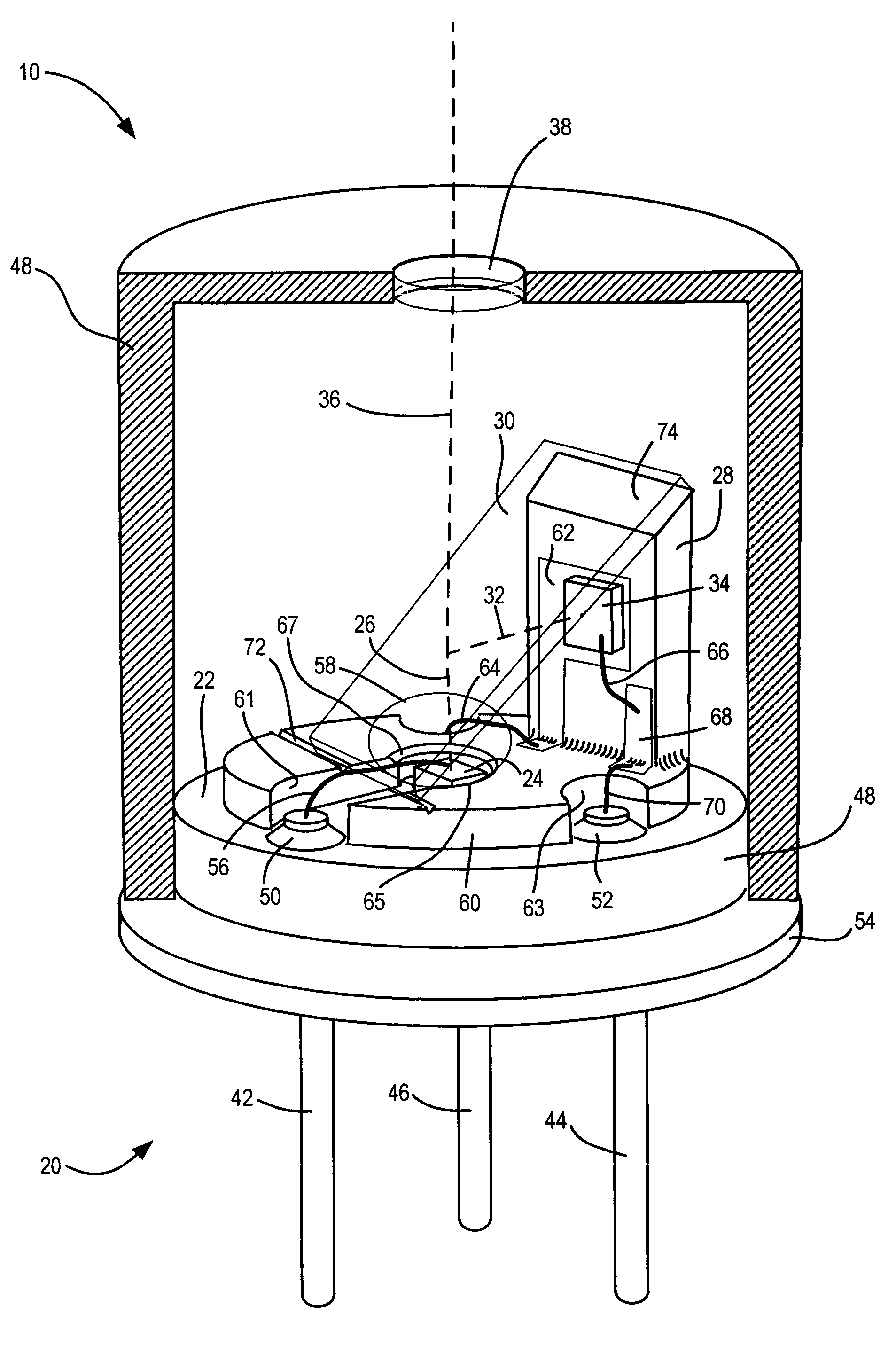
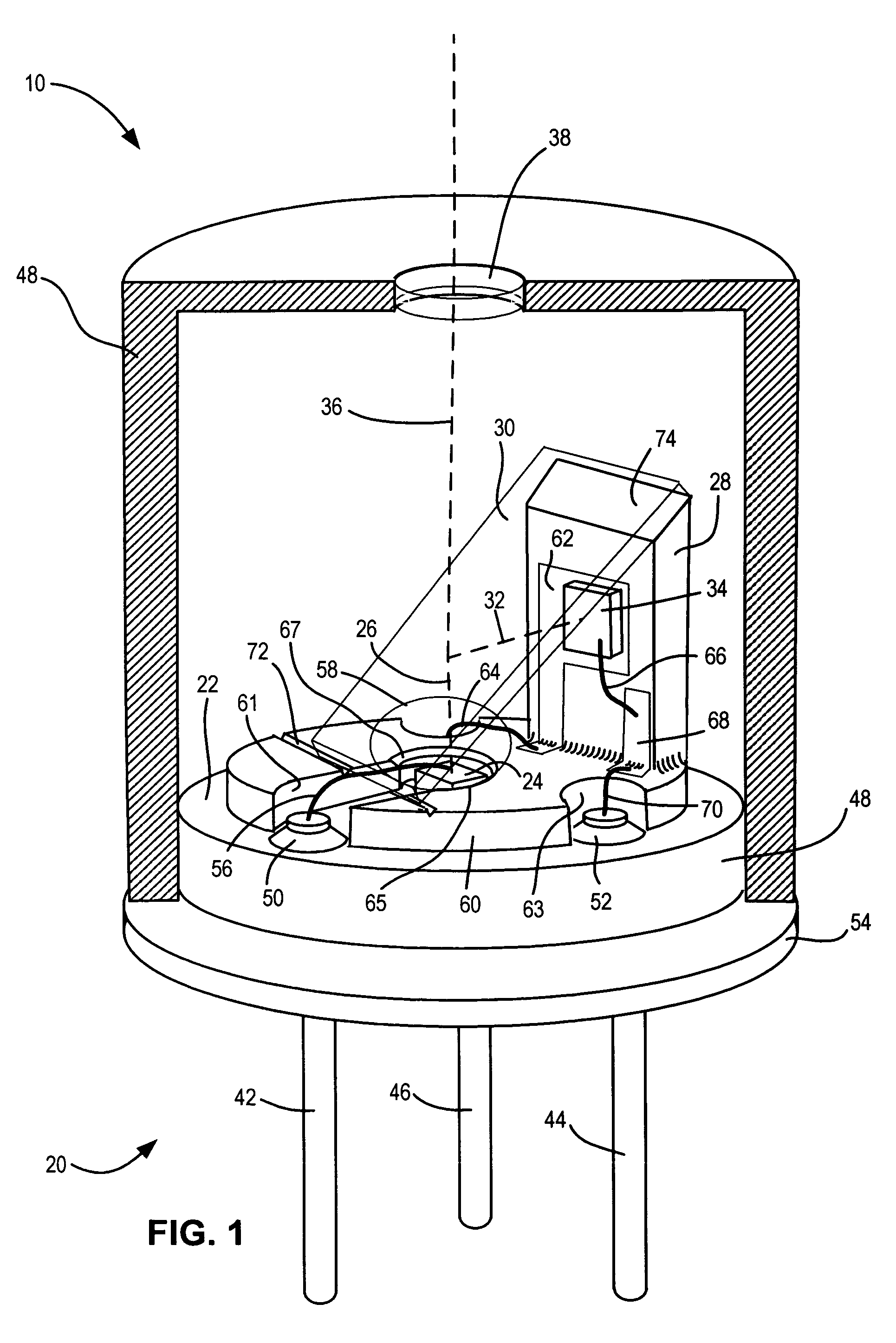
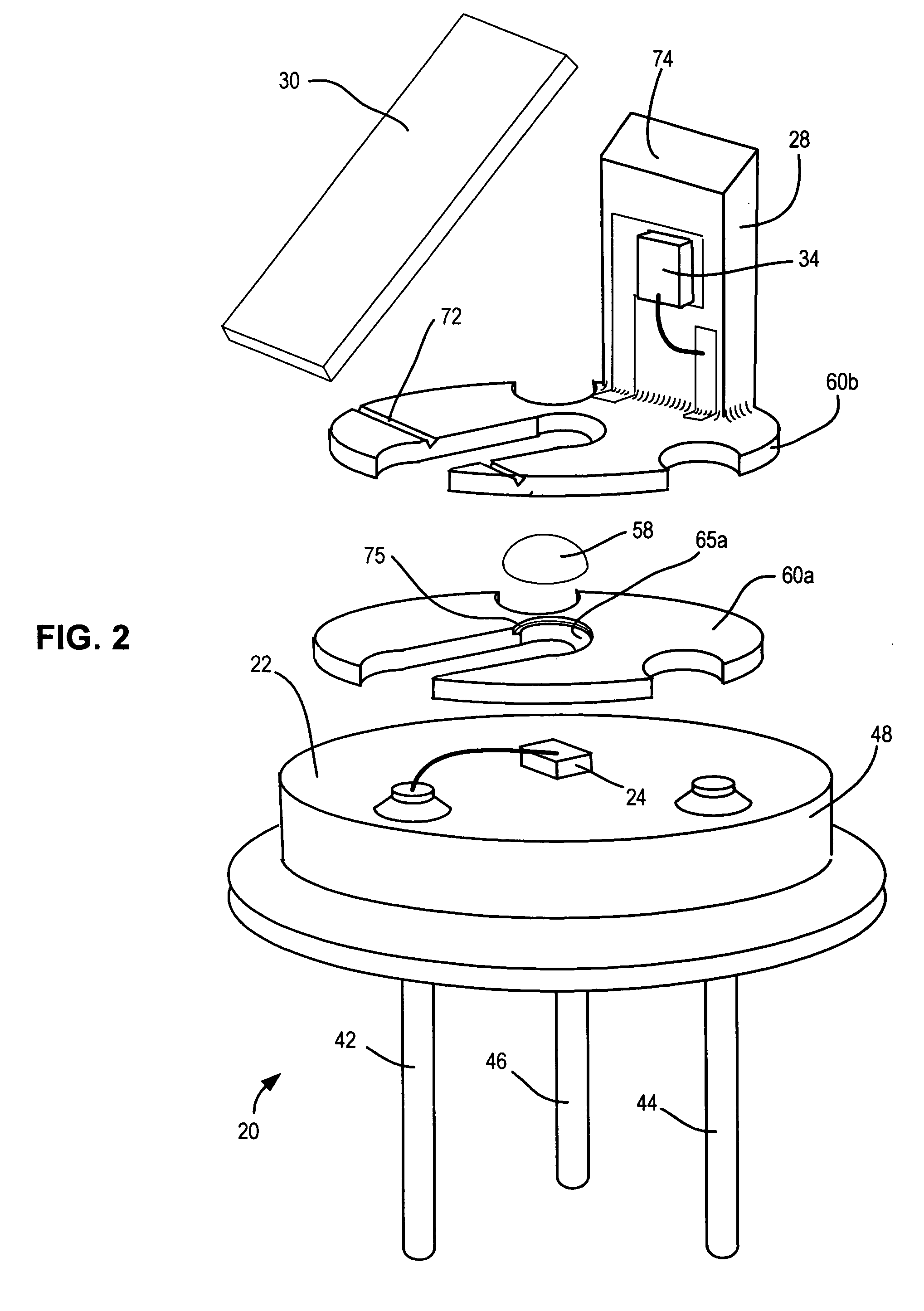
[0024] As shown in FIG. 1, one embodiment of a semiconductor light source unit 10 with optical feedback includes a header 20 having an upper horizontal surface 22 upon which is mounted a light-emitting element 24 for projecting a vertical beam of light 26. A vertical member 28 extends upward parallel to the beam 26. A beam splitter 30 is supported at least on one end by the vertical member 28 and extends over the light-emitting element 24 for reflecting a portion of the beam 26 to form a beam portion 32 which is transverse to the beam 26. A light-sensing element 34 is mounted on vertical member 28 for receiving the transverse beam portion 32. The light-sensing element 34 is mounted so that its acceptance cone is oriented at about 90° to the light beam 26 and so the active light sensing region of the light-sensing element receives substantially all of the transversely reflected beam portion 32. The non-reflected portion 36 of the beam.26 passes through the beam splitter 30 and a wind...


PUM


Abstract

A semiconductor light source with optical feedback includes a vertical member extending upward from an upper horizontal surface of a header parallel to a vertical beam projected from a semiconductor light-emitting element mounted on the horizontal surface of the header wherein the vertical member supports a light-sensing element for receiving light reflected transversely from the vertical beam by a beam splitter supported by the vertical member. The vertical beam passing through the beam splitter passes through a window or filter in a cap mounted on the header and covering the light-emitting element, the light-sensing element, the beam splitter, and the vertical member. Substantially all of the transversely reflected light impinges on the light-sensing element and can be used to control the power to the light-emitting element. A simple lens can by used to collimate the beam. Interior portions of the unit are formed from light absorbing materials such as black ceramic, black plastic, anodized aluminum, etc. The combined effect of the non-reflective interior of the assembly, the orientation of the photo-diode to have an acceptance cone perpendicular to the beam axis, the small entrance pupil, and the optical filter reduces ambient radiation in the unit by as much as −75 dB of the level outside the device. This reduces noise and drift in the automatic power control loop to produce constant intensity in the output light beam.

Description

BACKGROUND OF THE INVENTION [0001] Semiconductor light sources, including: light-emitting diodes (LED), infrared-emitting diodes (IRED), edge-emitting laser diodes (LD) and vertical-cavity, surface-emitting lasers (VCSEL), are used in most data-transmission and storage systems and in many sensors for measuring gas and fluid properties and detecting proximity and distance. Light emission is stimulated by passing an electrical current through the semiconductor. The efficiencies of these sources, expressed in Watts (W) of light power per Ampere (A) of excitation current (for one W of output at 25° C.), range from about 0.03 for LDs to 0.2 for VCSELs. Light-emitting diodes and IREDs emit incoherent light from all sides of the semiconductor chip and therefore required reflective packaging and collimating optics to direct the emitted light toward transmission devices or fluid samples. A typical laser diode has a semiconductor chip with reflecting front and back facets. Lasing causes emiss...

Claims


Application Information

Patent Timeline
Patent Type & Authority Applications(United States)
IPC IPC(8): G01J1/32
CPCG01J1/02G01J1/0204G01J1/4257G01J1/08G01J1/32G01J1/0414
Inventor DOWNING, JOHN P. JR.
Owner USL TECH
Why Eureka
Try Eureka