
Shared redundant memory architecture and memory system incorporating same

Active Publication Date: 2007-02-15
SK HYNIX INC
View PDF8 Cites 2 Cited by
  • Summary
  • Abstract
  • Description
  • Claims
  • Application Information

AI Technical Summary

Benefits of technology

[0010] To obviate the drawbacks of the prior art the object of the instant invention is to provide memory system incorporating shared redundant memories and shared redundant memory architecture. A further object of the instant invention is to provide memory system to reduce area overhead for the fuse and redundant memory. Another object of the instant invention is to provide a memory system to eliminate the redundancy effects on the memory timing characteristics.

Problems solved by technology

The increasing complexity of systems and semiconductor process is resulting in more defects in the System On Chip (SoC) design process.
Due to such a large presence of memories on chip, the chip yield is directly linked to the memory yield and hence to the memory defect level.
In the newer technologies the degree of defects in the memories have increased to a great extent due to shrinking dimensions.
In this context neither controlled process nor design can help in improving the SoC's yield as shrinking gate lengths have resulted in newer processes where the defect levels have gone beyond the control of the process and design.
The problem with using the type-1 redundancy in memory system is that it results in modified timing characteristics (setup / hold / access / cycle).
This type of redundancy also results in increased development cycle time for the memory compilers.
For instance, it is observed that the column redundancy leads to increased repair time for the memory after power on.
The problem with the type-2 redundancy is seen in terms of the memory performance as the soft routed memories can be routed all round the SoC which results in unnecessary routing congestion.
Also soft memories cannot be used for multi port memories as considerably more effort is required in designing multiport soft memories.
Even in a case where a hard memory of same type is used instead of the soft memory, there is a significant area overhead as besides the storage elements other logic blocks in a memory like address decoders, I / O sections etc. are also duplicated.
At system level, memory redundancy results in another problem when there are several small memories on a chip.
But not all the memories fail on a wafer and it is observed that most of the time the redundant memories are wasted.
Therefore putting redundancy for each memory is highly inefficient as it increases the overhead in terms of the memory area and fuse area and results in timing overhead as well.

Method used


Image

  • Shared redundant memory architecture and memory system incorporating same
  • Shared redundant memory architecture and memory system incorporating same
  • Shared redundant memory architecture and memory system incorporating same

Examples


Embodiment Construction

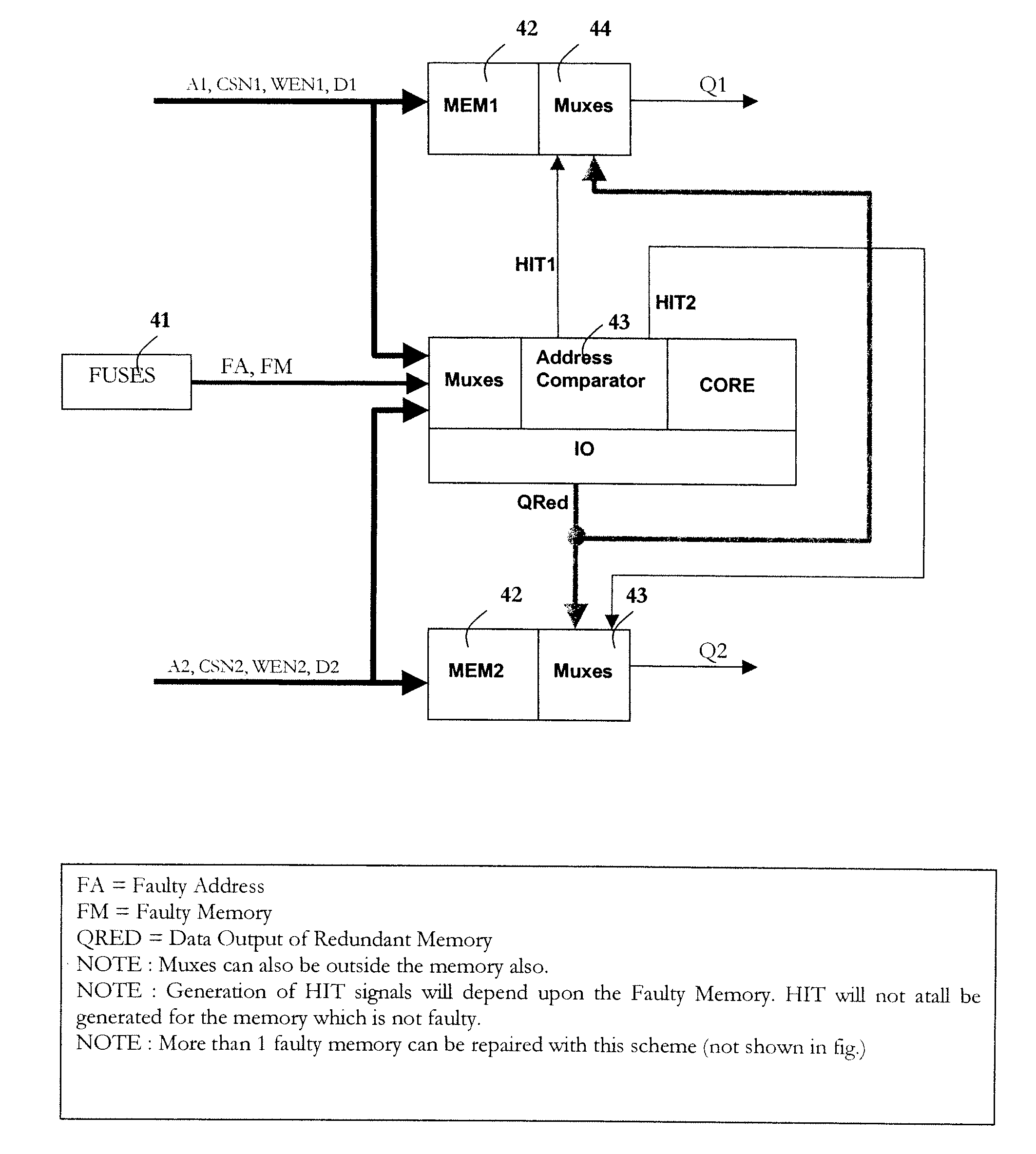
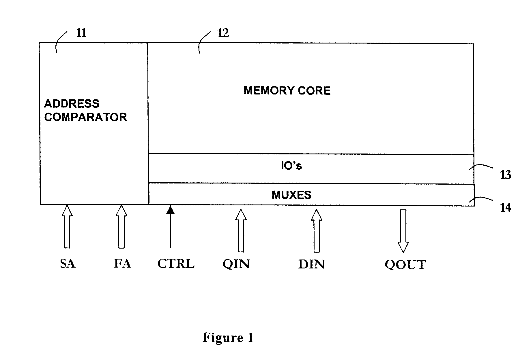
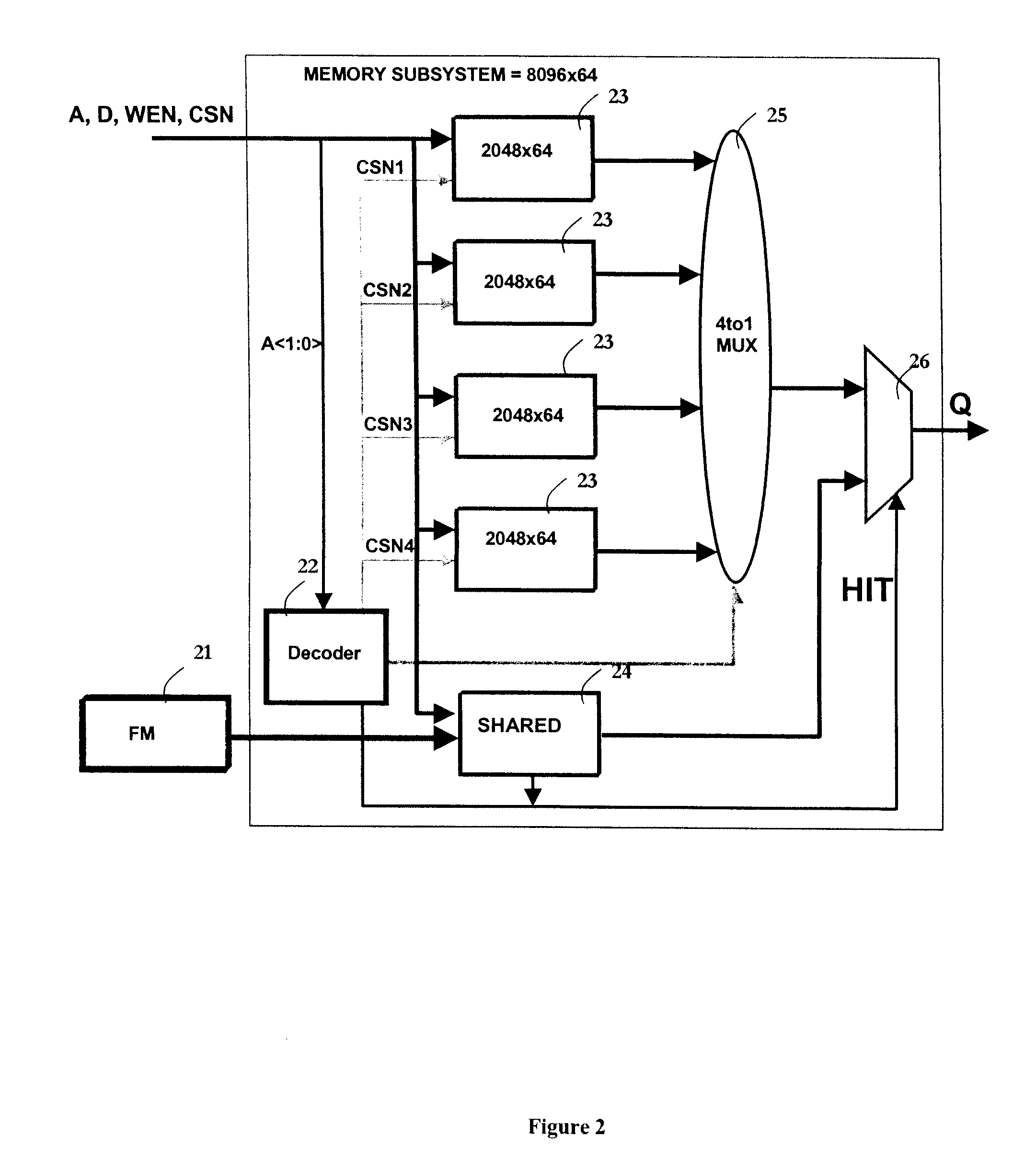
[0018] The current invention provides new high-speed memory system with modified redundant memories which are shared between various memories on a chip. Additionally, in the present invention, two different embodiments of shared redundant memory are provided for use depending on the memory systems on the chip. These memory systems can be categorized as follows: [0019] 1. Type-1 memory systems: In type-1 memory system, there are several small memories combined together to form a single large memory. [0020] 2. Type-2 memory systems: In type-2 memory system, there are several unrelated memories for different purposes located in close proximity of each other.

[0021] In both type-1 and type-2 systems, redundant memories are added to the system for purpose of repairing. The repair methodology / architecture is different from the existing techniques as the redundant memory is shared between various memories present on a SoC. However in order to henceforth differentiate normal memories from r...


PUM


Abstract

A memory system incorporates shared redundant memories and has a shared redundant memory architecture. The memory system includes a modified memory to be used as a shared redundant memory between memory systems. These memory systems may have several smaller memories forming a single logical memory or various memories in close proximity on an integrated circuit system. The shared redundancy is achieved by adding a comparator to the redundant element for comparing between the faulty address and the system address and performing a memory operation based on the comparator output. As the redundant memory operations are performed in parallel to the memory structures, setup and hold times are reduced. Shared redundancy also results in reduced integrated circuit area.

Description

RELATED APPLICATION [0001] The present invention claims priority of India Patent Application No. 2023 / Del / 2005 filed Jul. 29, 2005, which is incorporated herein in its entirety by this reference. FIELD OF THE INVENTION [0002] The present invention discloses a shared redundant memory architecture and memory system incorporating the same. Further, it also describes two different memory systems incorporating the redundant memory. BACKGROUND OF THE INVENTION [0003] The increasing complexity of systems and semiconductor process is resulting in more defects in the System On Chip (SoC) design process. The yield of these SoCs is directly linked to the memories on the SoC as around 60-70% of the silicon area on the chip is covered by the memories. Different types of memories are used for various operations on chips, like storage, temporary calculations, synchronization, buffering etc. Due to such a large presence of memories on chip, the chip yield is directly linked to the memory yield and ...

Claims


Application Information

Patent Timeline
IPC IPC(8): G11C29/00G11C7/00
CPCG11C29/846G11C29/808
Inventor DUBEY, PRASHANT
Owner SK HYNIX INC
Learn More