
Liquid crystal display device

a liquid crystal display and display device technology, applied in non-linear optics, instruments, optics, etc., can solve the problems of inability to realize compact liquid crystal display devices with a small panel size, difficult to lower the uneven display, etc., to achieve the effect of reducing resistance, improving display quality, and reducing resistance of common signal lines

Active Publication Date: 2007-02-08
TRIVALE TECH
View PDF4 Cites 33 Cited by
  • Summary
  • Abstract
  • Description
  • Claims
  • Application Information

AI Technical Summary

Benefits of technology

[0014] The present invention has been accomplished in view of the above problems, and it is accordingly an object of the invention to provide a liquid crystal display device that enables high display quality.
[0015] A liquid crystal display device according to a first aspect of the invention includes: a wiring substrate; an opposing substrate opposite to the wiring substrate; a sealing member for bonding the wiring substrate to the opposing substrate; a liquid crystal filled in a space defined by the wiring substrate, the opposing substrate, and the sealing member; a plurality of scanning signal lines formed in a display area formed inside the sealing member; a plurality of display signal lines formed in the display area and crossing the scanning signal lines through an insulating film; and a common signal line formed outside the display area, the scanning signal lines, the scanning signal lines, and common signal line being formed on the wiring substrate, and the common signal line including at least two conductive layers with one of the conductive layers changing a pattern width below a pattern of the sealing member. Thus, a resistance of the common signal line can be lowered with no abrupt change in panel gap, making it possible to improve display quality.
[0016] According to a second aspect of the invention, in the liquid crystal display device according to the first aspect, the common signal line below the pattern of the sealing member extends along one side of the sealing member, and the pattern width of the conductive layer is changed in a direction in which the common signal line extends. Thus, a delay of a common signal can be suppressed.

Problems solved by technology

Thus, a change in panel gap occurs due to the step at the corner of the image display portion, and causes an uneven display.
It is difficult to lower the resistance of the common signal line.
As a result, a frame area increases, resulting in a problem in that a compact liquid crystal display device with a small panel size cannot be realized.
In this case, the uneven display is caused due to the abrupt change in panel gap at the portion concerned.
Accordingly, in the structure of FIG. 14, a region where the two-layer line can be formed is limited for avoiding the abrupt change in panel gap.
In some cases, this hinders the reduction in resistance necessary for high-speed driving.
As mentioned above, in the conventional liquid crystal display device, the uneven display is caused due to the abrupt change in panel gap, so the resistance of common signal line cannot be lowered.
This leads to a problem in that the uneven display is caused, and display quality cannot be improved.
As discussed above, a conventional display device faces a problem in that, if the resistance of the common signal line is lowered, the uneven display is caused due to the abrupt change in panel gap, and the display quality cannot be improved.

Method used


Image

  • Liquid crystal display device
  • Liquid crystal display device
  • Liquid crystal display device

Examples


first embodiment

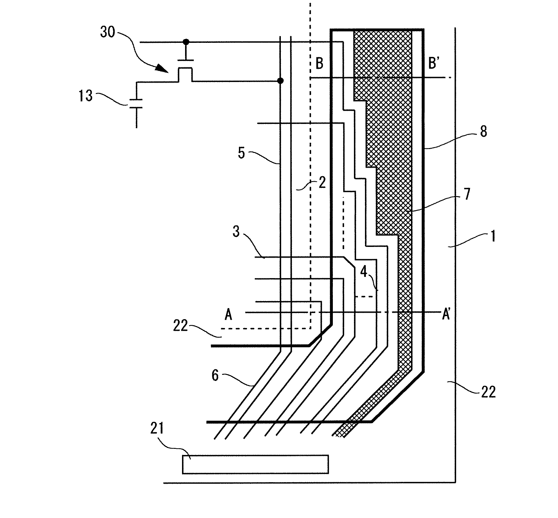
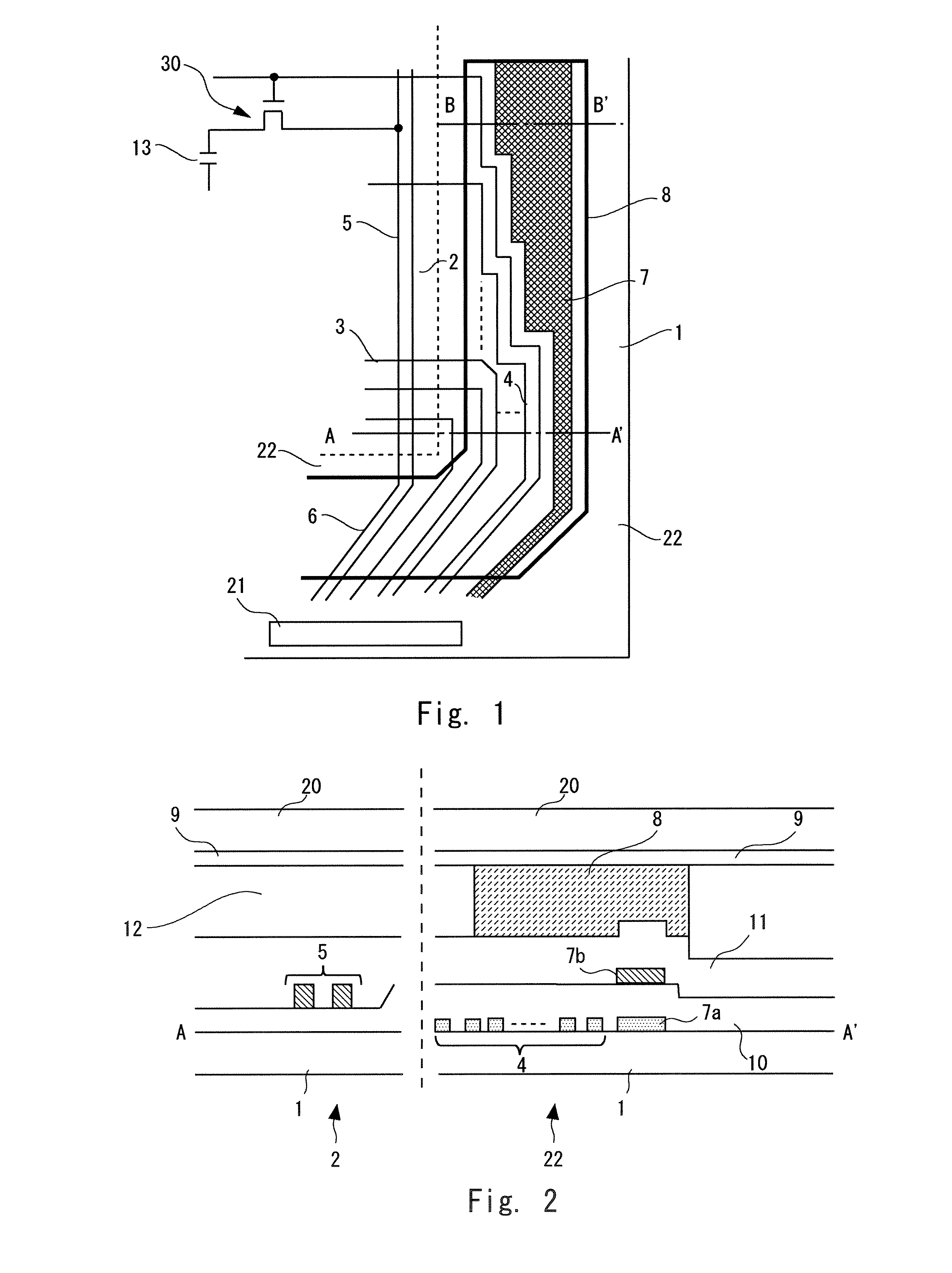
[0044] Referring to FIGS. 1 to 3, a liquid crystal display device according to a first embodiment is described. FIG. 1 is a plan view showing the structure of an end portion of a wiring substrate used in the liquid crystal display device of this embodiment. Incidentally, FIG. 1 shows the structure of a lower-right corner portion of a sealing member formed on the wiring substrate. FIG. 2 is a sectional view showing the structure of a liquid crystal display panel taken along the line A-A′ of FIG. 1. FIG. 3 is a sectional view showing the structure of the liquid crystal display panel taken along the line B-B′ of FIG. 1. In FIGS. 1 to 3, reference numeral 1 denotes a wiring substrate; 2, a display area; 3, a scanning signal line; 4, a scanning signal lead-out line connected with the scanning signal line; 5, a display signal line; 6, a display signal lead-out line connected with the display signal line; 7, a common signal line; 8, a sealing member; 9, a counter electrode; 10, a gate insu...

second embodiment

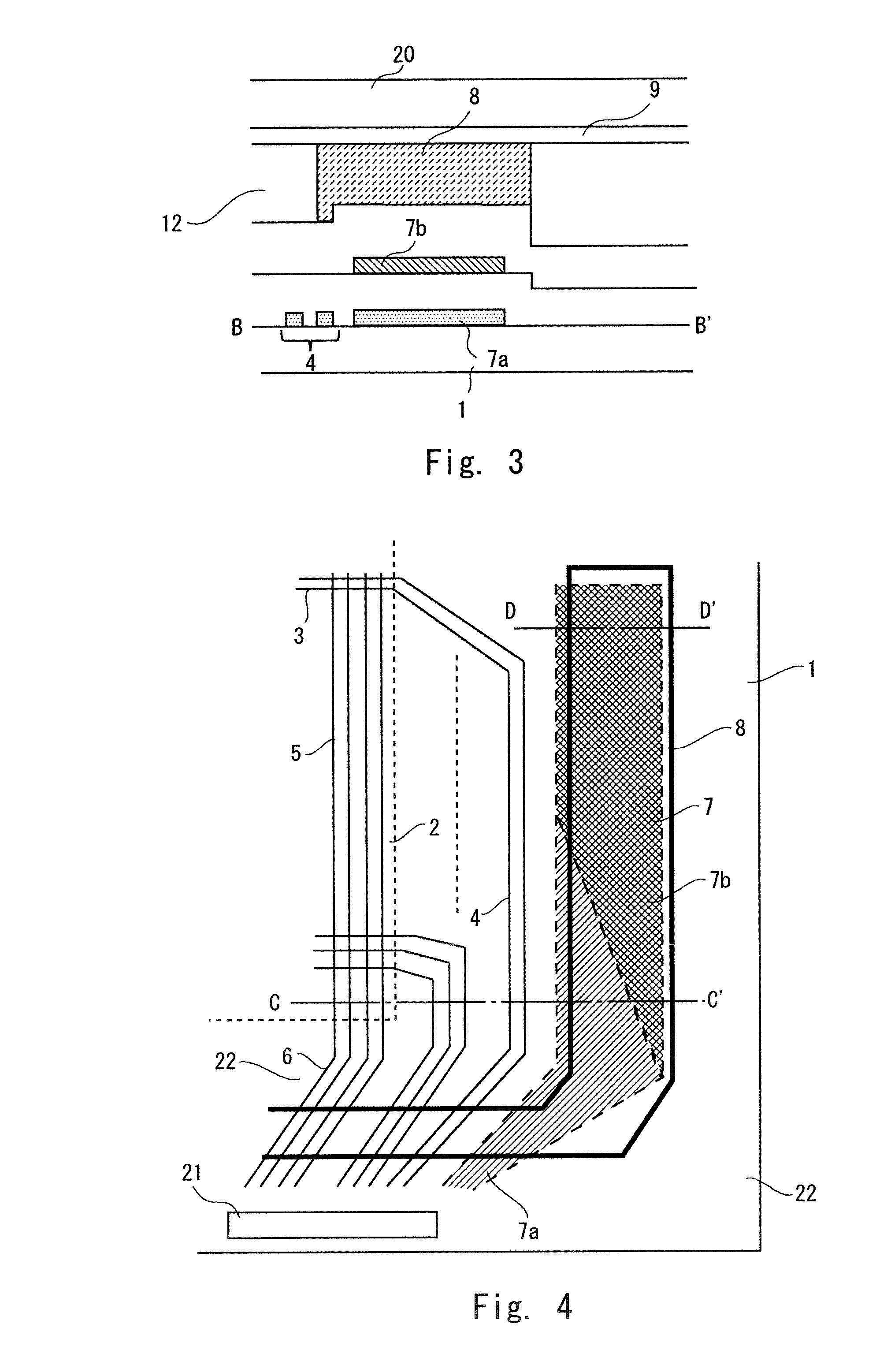
[0064] Referring to FIGS. 4 to 6, the structure of a liquid crystal display device according to a second embodiment of the present invention is described. FIG. 4 is a plan view showing the structure of an end portion of a wiring substrate used in the liquid crystal display device of this embodiment. Incidentally, FIG. 4 shows the structure of the lower-right corner portion of the sealing member in the wiring substrate. FIG. 5 is a sectional view showing the structure of the liquid crystal display panel taken along the line C-C′ of FIG. 4. FIG. 6 is a sectional view showing the structure of the liquid crystal display panel taken along the line D-D′ of FIG. 4. The basic structure of the wiring substrate of this embodiment is the same as the first embodiment, so detailed description thereof is omitted. Further, description about the same components as those of the first embodiment is omitted.

[0065] In this embodiment, the scanning signal lead-out line 4 is formed inside the pattern of...

third embodiment

[0072] Referring to FIGS. 7 and 8, the structure of a liquid crystal display device according to a third embodiment of the present invention is described. FIG. 7 is a plan view showing the structure of an end portion of a wiring substrate used in the liquid crystal display device of this embodiment. Incidentally, in FIG. 7, the structure of the lower-right corner portion of the sealing member in the wiring substrate is demonstrated. FIG. 8 is a sectional view showing the structure of the liquid crystal display panel taken along the line E-E′ of FIG. 7. Incidentally, the basic structure of the wiring substrate of this embodiment is the same as that of the first embodiment, so detailed description thereof is omitted. Furthermore, description about the same components as those of the first embodiment is omitted.

[0073] In this embodiment, the pattern shape of the common signal line 7 provided outside the scanning signal lead-out line 4 is the same as that of the first embodiment. Furth...


PUM


Abstract

A liquid crystal display device according to an embodiment of the present invention includes: a wiring substrate; an opposing substrate opposite to the wiring substrate; a sealing member for bonding the wiring substrate to the opposing substrate; a liquid crystal filled in a space defined by the wiring substrate, the opposing substrate, and the sealing member; a plurality of scanning signal lines formed in a display area formed inside the sealing member; a plurality of display signal lines formed in the display area and crossing the scanning signal lines with an insulating film interposed therebetween; and a common signal line formed outside the display area, the scanning signal lines, the scanning signal lines, and common signal line being formed on the wiring substrate, and the common signal line including at least two conductive layers with one of the conductive layers changing a pattern width below a pattern of the sealing member.

Description

BACKGROUND OF THE INVENTION [0001] 1. Field of the Invention [0002] The present invention liquid crystal display device. In particular, the invention relates to a liquid crystal display device having a common signal line provided on a substrate. [0003] 2. Description of Related Art [0004] In general, liquid crystal display devices are structured such that a pair of upper and lower electrode substrates having transparent electrodes are bonded to each other by use of a sealing member formed around an image display portion of the substrate and liquid crystal is filled therein. The liquid crystal display devices are classified into an active matrix type and a passive matrix type. An active matrix type liquid crystal display device as disclosed in Japanese Unexamined Patent Application Publication No. 11-149087 has a TFT array substrate where thin film transistors as switching elements are arranged in matrix (see Japanese Unexamined Patent Application Publication No. 11-149087). Then, th...

Claims


Application Information

Patent Timeline
IPC IPC(8): G02F1/1333
CPCG02F1/1345G02F2001/133388G02F1/136286G02F1/133388
Inventor AOKI, HIRONORI
Owner TRIVALE TECH
Learn More