
Flexible printed circuit and display device using the same

a printed circuit and display device technology, applied in the direction of fixed connections, instruments, optics, etc., can solve the problems of display device defects, electrode terminal disconnection, erosion or corrosion,

Active Publication Date: 2007-01-18
TRIVALE TECH
View PDF1 Cites 54 Cited by
  • Summary
  • Abstract
  • Description
  • Claims
  • Application Information

AI Technical Summary

Benefits of technology

[0011] An object of the present invention is to provide a flexible printed circuit that is less likely to suffer from erosion (corrosion) of electrode terminals even in severe environments and a display device using the flexible printed circuit.
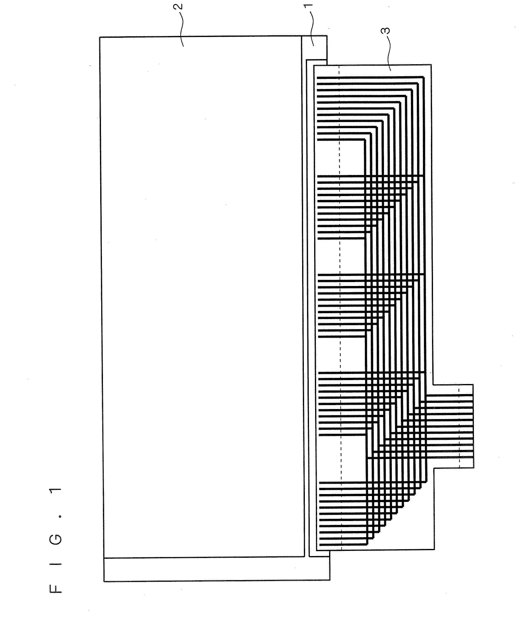
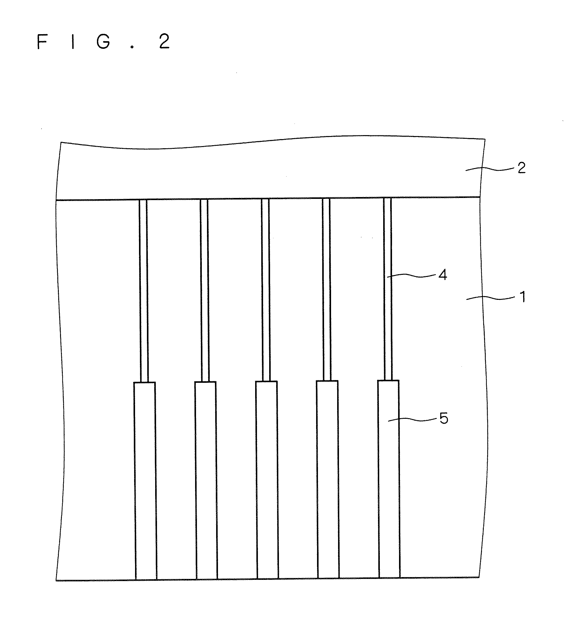
[0013] According to the flexible printed circuit of the invention, the ends of terminals are located inside an outline of the insulative film. Accordingly, when the terminals are connected to external electrode terminals, the insulative film covers the connections so that the electrode terminals are less likely to suffer from erosion (corrosion) even in severe environments.
[0015] The display device of the invention is less likely to suffer from erosion (corrosion) of the electrode terminals even in severe environments, which reduces inferior displays and enhances reliability.

Problems solved by technology

However, when such a display device undergoes a reliability test in a severe environment, e.g., in a hot and humid environment, water may penetrate the insulative coating material to invade the ACF.
When water invades the ACF, higher-potential electrode terminals may corrode away as minus ions in areas where the higher-potential electrode terminals are placed adjacent to lower-potential electrode terminals, which results in disconnection of the electrode terminals (the phenomenon called erosion or corrosion).
The disconnection of electrode terminals stops supply of desired signals to pixels and then the display device suffers from display defects.

Method used


Image

  • Flexible printed circuit and display device using the same
  • Flexible printed circuit and display device using the same
  • Flexible printed circuit and display device using the same

Examples


Embodiment Construction

[0029] (First Preferred Embodiment)

[0030] First, prior to the description of the flexible printed circuit according to a first preferred embodiment, a common flexible printed circuit will now be described. FIG. 9 is a plan view of a common flexible printed circuit. The flexible printed circuit of FIG. 9 includes FPC input terminals 101 and FPC terminals 103 connected thereto through FPC interconnections 102. In the flexible printed circuit shown in FIG. 9, the FPC terminals 103 are provided in five areas, while the FPC input terminals 101 are provided in one area.

[0031]FIG. 10A is a plan view of an area where FPC terminals 103 reside, and FIG. 10B is a cross-sectional view of the area including the FPC terminals 103. As shown in FIG. 10B, the flexible printed circuit includes an FPC film 104 having a thickness of about 30 μm to 70 μm, FPC interconnections 102 and FPC terminals 103 having a thickness of about 8 μm to 25 μm, and a polyimide-based solder resist 105 covering the FPC i...


PUM

PropertyMeasurementUnit
thicknessaaaaaaaaaa
thicknessaaaaaaaaaa
temperatureaaaaaaaaaa

Abstract

The present invention provides a flexible printed circuit that is less likely to suffer from erosion (corrosion) of electrode terminals even in severe environments and a display device using the flexible printed circuit. According to the present invention, a flexible printed circuit includes a flexible FPC film, FPC interconnections formed of a given pattern on the FPC film, a solder resist covering the FPC interconnections, and FPC terminals provided at ends of the FPC interconnections to make external connection. According to the invention, the FPC terminals include at least one terminal that has an end located inside of an outline of the FPC film.

Description

BACKGROUND OF THE INVENTION [0001] 1. Field of the Invention [0002] The present invention relates to flexible printed circuits and display devices using the same, and particularly to the structure of terminals of a flexible printed circuit that are connected to electrode terminals of a display panel. [0003] 2. Description of the Background Art [0004] A conventional liquid-crystal display device includes two glass substrates with liquid crystal sandwiched therebetween, driver circuitry connected to interconnections on the glass substrates, and an illumination device placed on the back of the glass substrates. Particularly, in a liquid-crystal display device using thin film transistors (TFTs), the TFTs are arranged in a matrix on one glass substrate, and an opposing electrode is formed on the other glass substrate. Also, electrode terminals are provided in the peripheral area of the one glass substrate in order to connect interconnections extending from the TFTs to the driver circuitr...

Claims


Application Information

Patent Timeline
Patent Type & Authority Applications(United States)
IPC IPC(8): G02F1/1345
CPCG02F1/13452G02F2001/133388H01R4/04H01R12/62H05K1/117H01R12/7076H05K3/323H05K3/361H05K2201/091H05K2201/09145H05K3/284G02F1/133388H05K1/02
Inventor WATANABE, KENICHIUEDA, HIROSHITACHIBANA, HIROSHINOUMI, SHIGEAKI
Owner TRIVALE TECH
Learn More