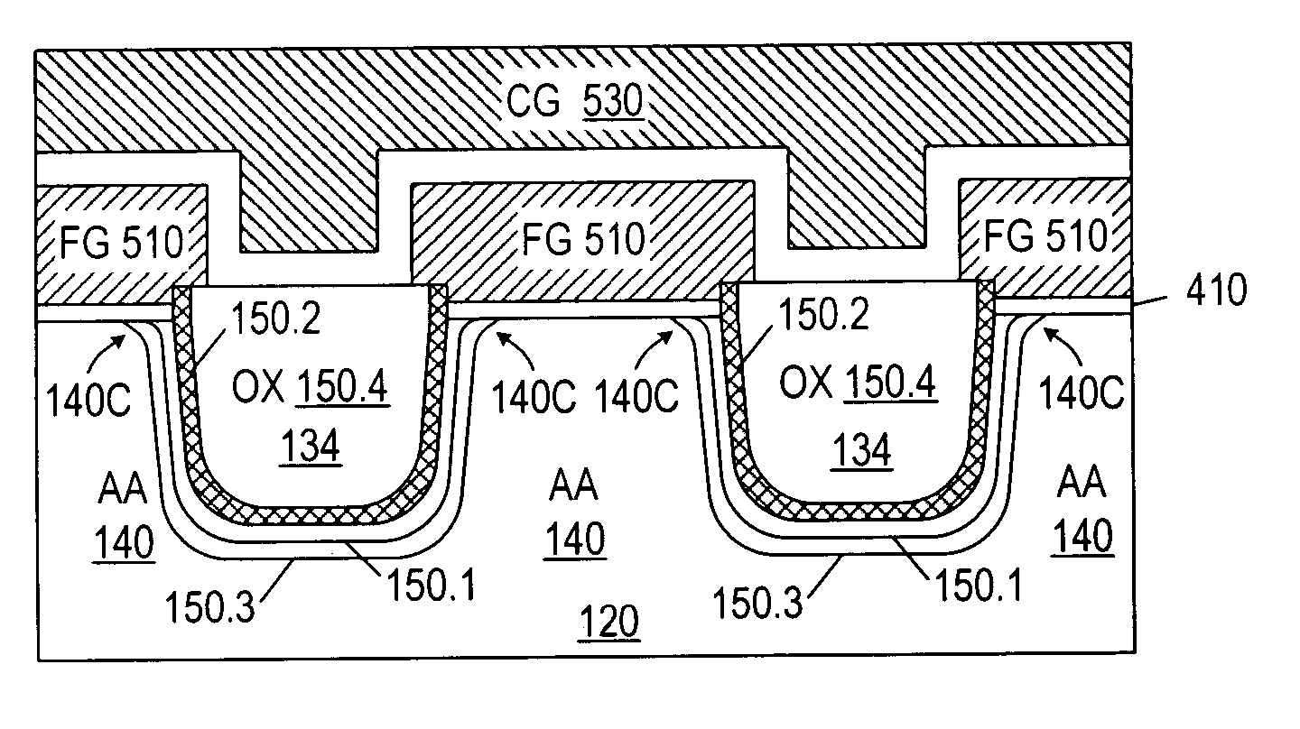
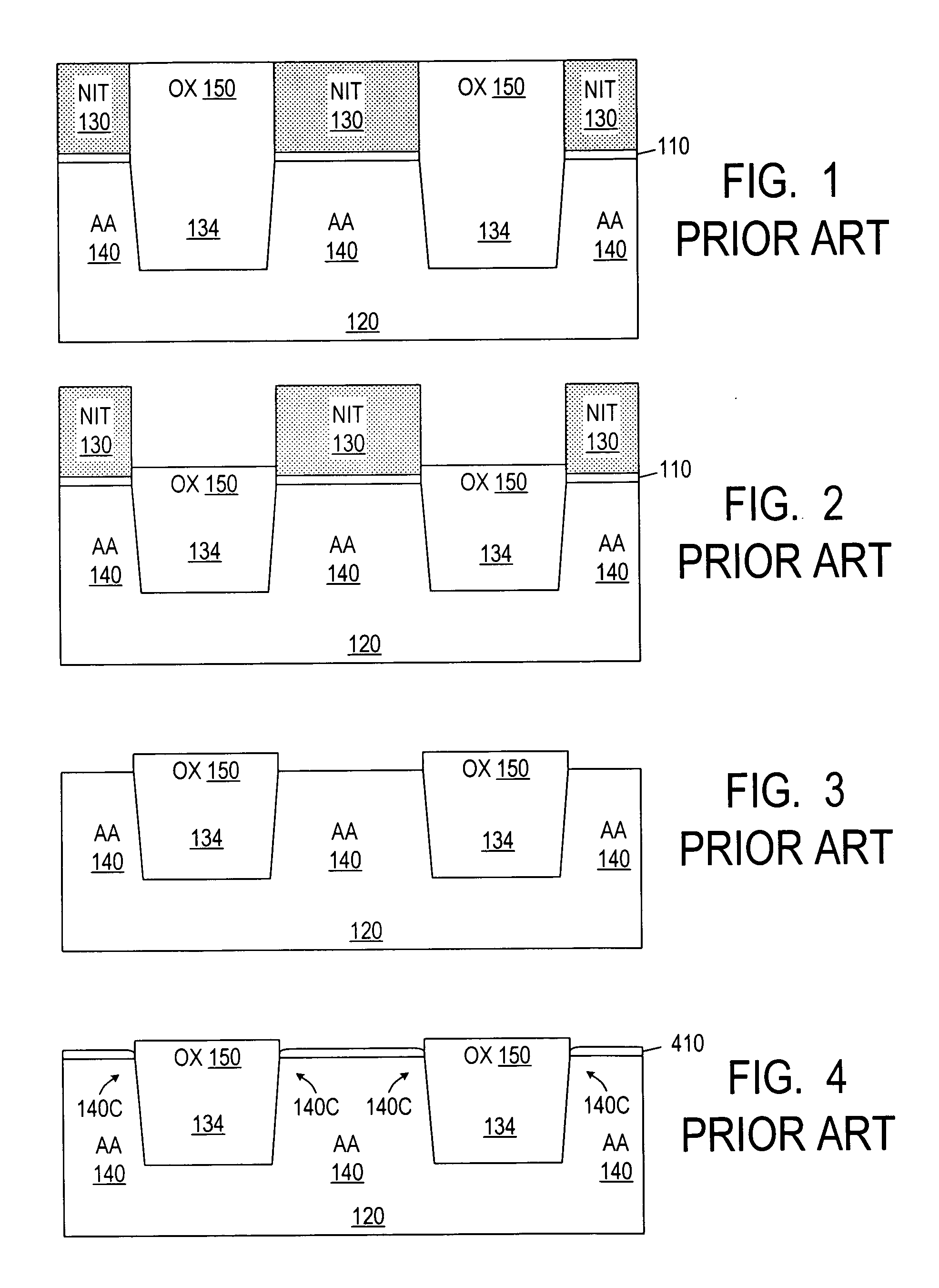
Use of chlorine to fabricate trench dielectric in integrated circuits
a dielectric and integrated circuit technology, applied in the field of integrated circuits, can solve problems such as overerase and/or other problems, and achieve the effects of preventing undue consumption of active area, reducing the oxidation time, and enhancing the corner rounding
- Summary
- Abstract
- Description
- Claims
- Application Information
AI Technical Summary
Benefits of technology
Problems solved by technology
Method used
Image
Examples
Embodiment Construction
[0016] The embodiments described in this section illustrate but do not limit the invention. The invention is not limited to particular fabrication techniques or numerical values and ranges. The invention is defined by the appended claims.
[0017]FIG. 9 illustrates initial ST1 fabrication stages in one embodiment of the present invention. Silicon dioxide layer 110 comprising chlorine atoms is formed on silicon wafer 120. In some embodiments, the chlorine concentration is more than three atomic percent, or at least 5 atomic percent. A range from 5 to 15 atomic percent is believed to be suitable, and other concentrations are possible.
[0018] In one embodiment, oxide 110 is formed by thermal oxidation at 800˜1000° C. The oxygen flow is 10±5 l / min (liters per minute). The chlorine is provided by hydrogen chloride (HCl) flown at 1 l / min. Other possible chlorine sources include the chlorine gas (Cl), TCA (trichloroethane, C2H3Cl3), TCE (trichloroethylene, C2HCl2), dichloroethylene (C2H2Cl2)...
PUM
 Abstract
Description
Claims
Application Information
 - R&D
- Intellectual Property
- Life Sciences
- Materials
- Tech Scout
- Unparalleled Data Quality
- Higher Quality Content
- 60% Fewer Hallucinations
Browse by: Latest US Patents, China's latest patents, Technical Efficacy Thesaurus, Application Domain, Technology Topic, Popular Technical Reports.
© 2025 PatSnap. All rights reserved.Legal|Privacy policy|Modern Slavery Act Transparency Statement|Sitemap|About US| Contact US: help@patsnap.com


