Nanocomposite for enhanced rectification
a technology of nanocomposites and rectification, which is applied in the field of enhanced band bending materials, can solve the problems of changing the structure of the band, the quality and performance of the device made from metal semiconductor contacts is poor, and the current fabrication methods and materials are near their theoretical limits, and achieves the effects of low cost, low cost, and improved quality and performan
- Summary
- Abstract
- Description
- Claims
- Application Information
AI Technical Summary
Benefits of technology
Problems solved by technology
Method used
Image
Examples
example 1
Formation of Nanocomposite
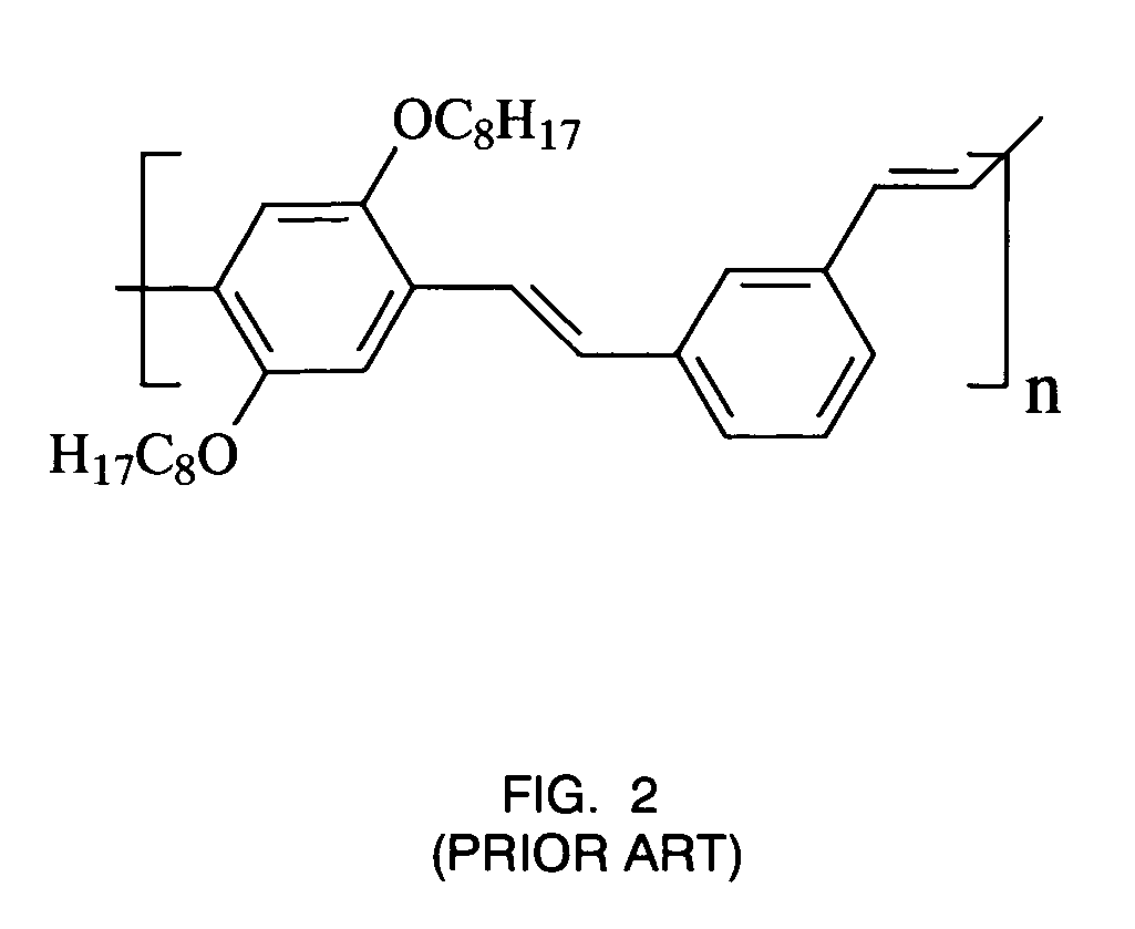
[0049] To form nanocomposites, gold nanoparticles were prepared by reducing aqueous tetrachloroaurate hydrate (1 mM, 250 mL) by slow addition of aqueous sodium borohydride (7 mM, 10.0 mL). A biphasic mixture was created by gently adding toluene (100 mL, HPLC grade) to the gold colloid solution, insuring no mixing. A 1 mL solution of poly(m-phenylenevinylene-co-2,5-dioctoxy-p-phenlenevinylene) (PmPV) (0.5 g / L in toluene, Aldrich) was added to the toluene layer and the biphasic mixture was stirred at 600 rpm for 5 minutes. After allowing the solution to settle into two layers, a fine bluish / violet suspension was formed at the interface in the toluene layer. This layer was separated off and the newly formed PmPV-gold nanocomposite was filtered out under vacuum to yield a nanocomposite of approximately 5% wt / wt gold to PmPV.
example 2
Characterization of the Nanocomposite
[0050] The individual cluster sizes were estimated using suspensions of the PmPV / gold nanoclusters in toluene in a quartz cell (1 cm path length), using a Perkin Elmer Lambda 20 UV-VIS spectrometer.
[0051] Raman spectra were obtained for drop cast pure PmPV and PmPV-gold nanocomposite, on silicon substrates, using a Renishaw InVia Raman spectrometer equipped with a Raman Leica RE02 microscope. A He / Ne and a diode laser were used for 633 nm and 785 nm excitation, respectively. Calibration was carried out using silicon at 520.5 nm.
[0052] A very thin film of the PmPV-Au nanocomposite was spun coat onto a glass cover slide using a Model WS-400A 6NPP / LITE spin coater. This thin film was then imaged using a Veeco Aurora-3 Near-field scanning optical microscope (NSOM) in transmission mode using a 632.8 nm He-Ne laser for the incident illumination. Thus, topographical as well as optical transmission images were obtained simultaneously.
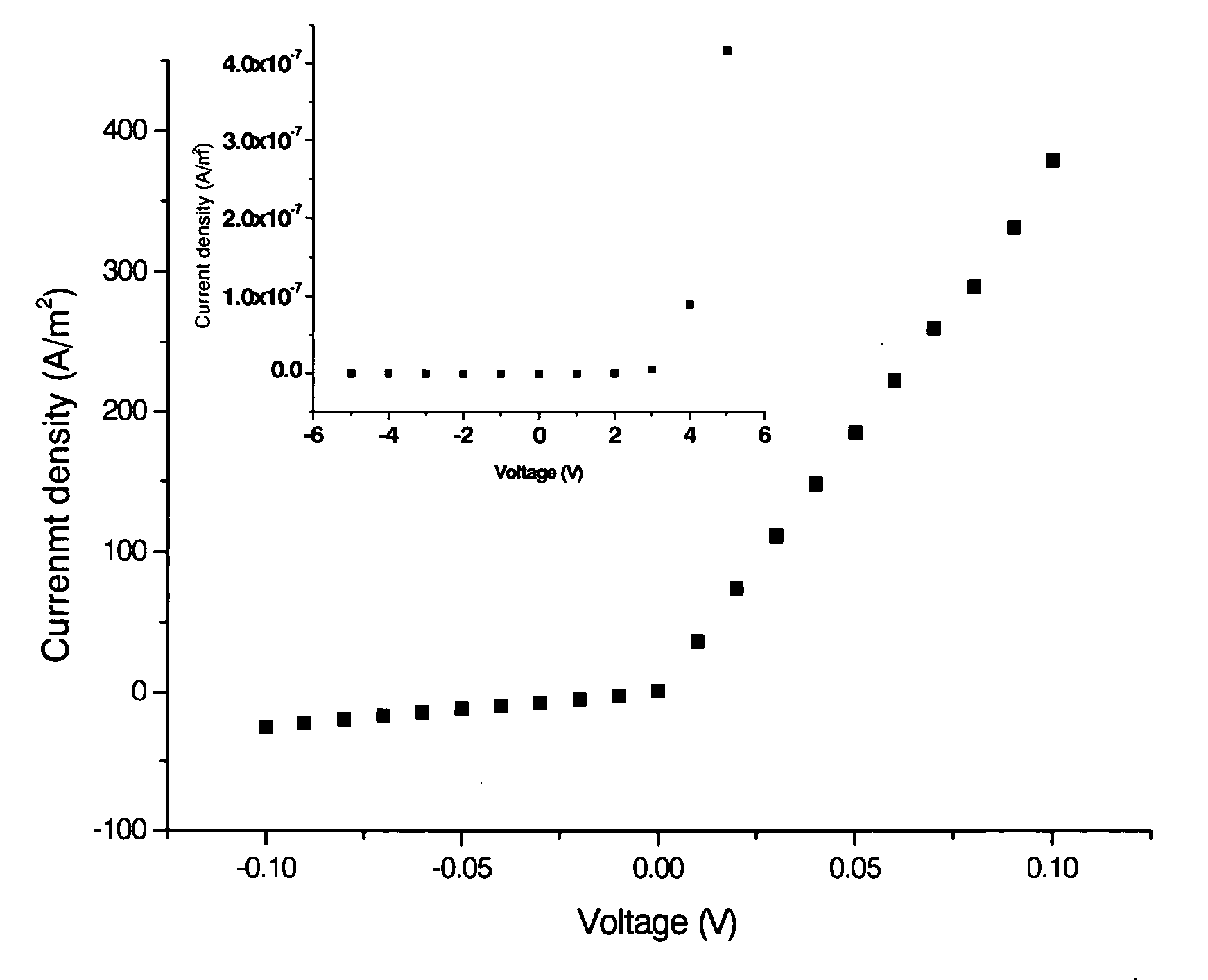
[0053] Sandwich ...
example 3
UV-Visible Spectroscopy
[0055] As shown in FIG. 3, distinct differences were observed in the 500-800 nm region between the gold colloid prior to, and then after, the addition of PmPV addition. As shown in the bottom spectrum in FIG. 3, the gold colloid prior to the addition of PmPV addition showed two surface plasmons located at 526 nm (2.36 eV) and 686 nm (1.81 eV). These two bands indicated a bimodal size distribution in the colloid, with the band at 526 nm corresponding to a particle size of approximately 20 nm and the band at 686 nm corresponding to particles in which inter-particular binding is occurring.
[0056] After addition of PmPV to the gold colloid biphasic mixture, the peak at 526 nm was broadened and red shifted by 0.11 eV, to 552 nm (2.25 eV). This drop in the gold nanoparticles Homo-Lumo gap is the result of an electron transfer process. Consequently, there was a shift to lower energy inflicted by the new charge transfer process, resulting in a decrease in the gold co...
PUM
| Property | Measurement | Unit |
|---|---|---|
| Size | aaaaa | aaaaa |
| Size | aaaaa | aaaaa |
| Size | aaaaa | aaaaa |
Abstract
Description
Claims
Application Information
 - R&D
- Intellectual Property
- Life Sciences
- Materials
- Tech Scout
- Unparalleled Data Quality
- Higher Quality Content
- 60% Fewer Hallucinations
Browse by: Latest US Patents, China's latest patents, Technical Efficacy Thesaurus, Application Domain, Technology Topic, Popular Technical Reports.
© 2025 PatSnap. All rights reserved.Legal|Privacy policy|Modern Slavery Act Transparency Statement|Sitemap|About US| Contact US: help@patsnap.com


