
Method and apparatus for arranging recipe of scanning electron microscope and apparatus for evaluating shape of semiconductor device pattern

a scanning electron microscope and semiconductor device technology, applied in material analysis using wave/particle radiation, instruments, nuclear engineering, etc., can solve the problem of not being able to select appropriate imaging points, and achieve the effect of rapid adaptation to process changes and easy establishmen

Inactive Publication Date: 2006-12-21
HITACHI HIGH-TECH CORP
View PDF1 Cites 37 Cited by
  • Summary
  • Abstract
  • Description
  • Claims
  • Application Information

AI Technical Summary

Benefits of technology

[0011] The present invention also provides a semiconductor pattern shape evaluation apparatus and method that can use the above-optimized imaging-recipe and SEM apparatus or the like to measure at high speed and accurately a large number of portions to be inspected, estimate semiconductor device characteristics and manufacturing process states, and feed back measurement and estimation results to various process sites.
[0016] According to the present invention, selection rules for automatic arrangement of an imaging recipe can be easily established by processing such as teaching or weight adjustment. It is therefore possible to rapidly accommodate changes in process where a wafer is manufactured, in process where a wafer is imaged, in imaging conditions, and in the like.

Problems solved by technology

Therefore, there has been the problem that appropriate imaging points cannot be selected because unbridgeable gulf of externals between the above linear image and an actual SEM image is large.

Method used


Image

  • Method and apparatus for arranging recipe of scanning electron microscope and apparatus for evaluating shape of semiconductor device pattern
  • Method and apparatus for arranging recipe of scanning electron microscope and apparatus for evaluating shape of semiconductor device pattern
  • Method and apparatus for arranging recipe of scanning electron microscope and apparatus for evaluating shape of semiconductor device pattern

Examples


Embodiment Construction

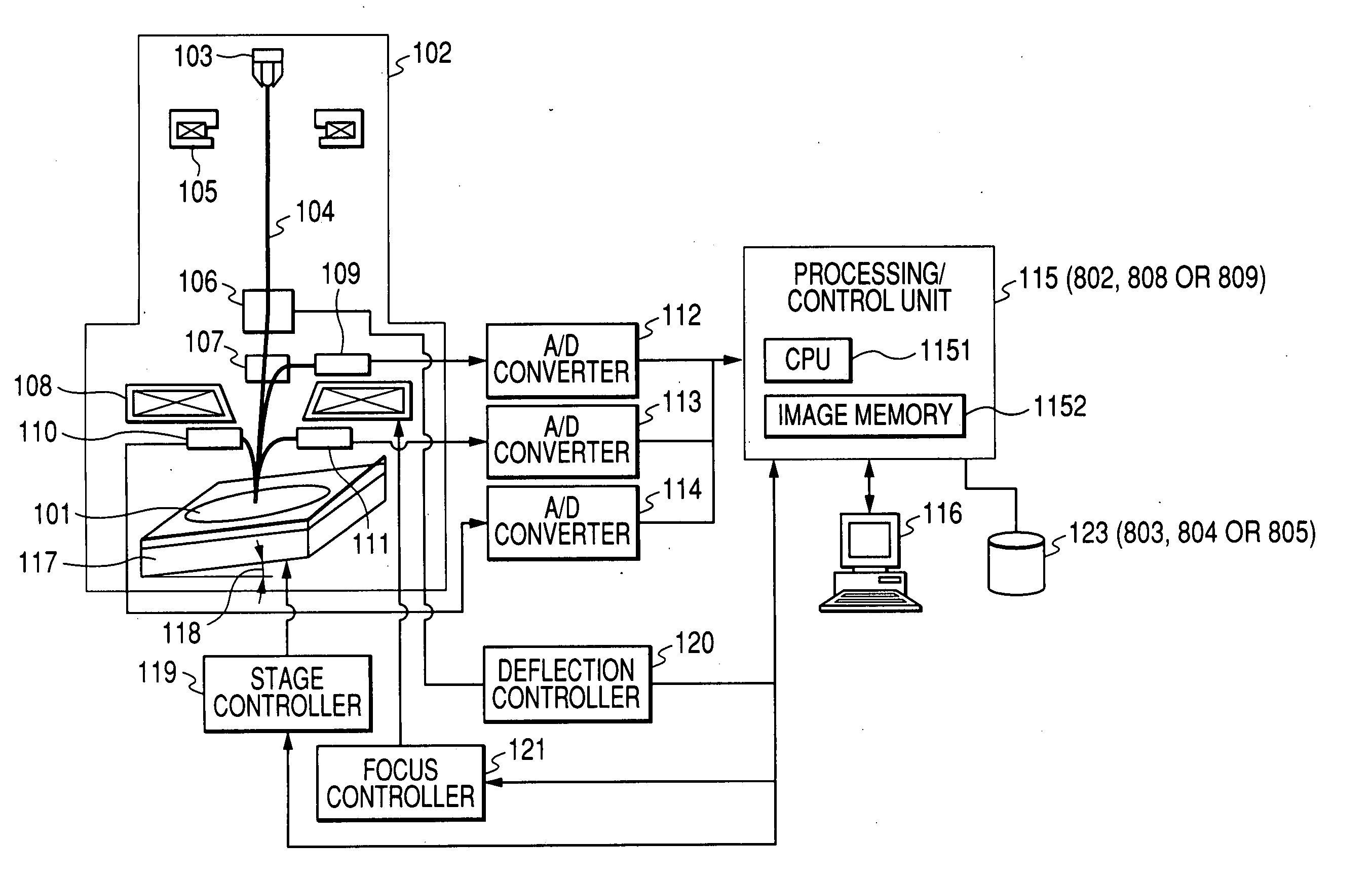
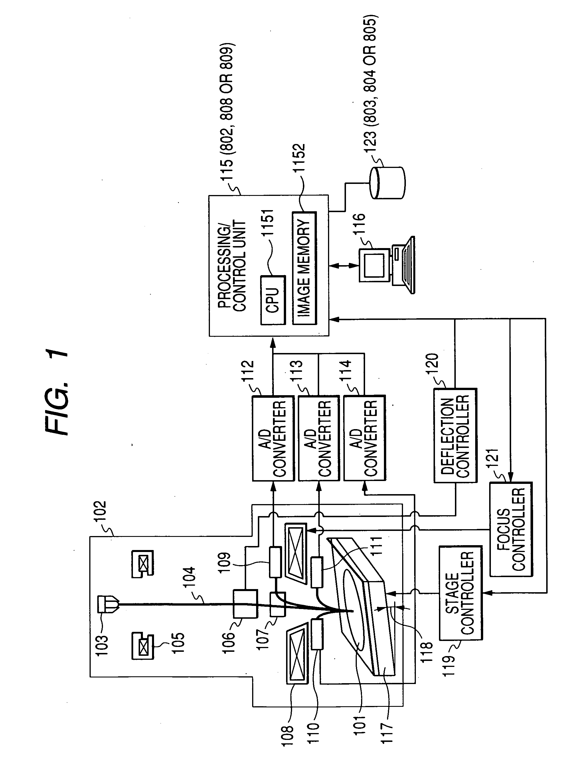
[0039] Embodiments of a SEM apparatus with an imaging recipe arrangement function according to the present invention, namely, a semiconductor pattern shape evaluation apparatus using a scanning electron microscope such as a critical-dimension scanning electron microscope (CD-SEM), will be described hereunder using FIGS. 1 to 12.

[0040] The number of inspection portions that require dimensional management of semiconductor patterns may be increasing greatly because of factors for such as decreases in design margins according to making minutely and making high density of LSI patterns. These tendencies are bringing about a strong demand for the improvement of the throughput and automation ratio of a SEM apparatus or like apparatus used as a dimensional management tool.

[0041] To use a SEM apparatus (or the like) for performing SEM-based observations for the critical points as dimension-measuring points on the semiconductor pattern to be inspected, and evaluating pattern shapes by measur...


PUM


Abstract

In order to provide an imaging-recipe arranging or creating apparatus and method adapted so that selection rules for automatic arrangement of an imaging recipe can be optimized by teaching in a SEM apparatus or the like, the imaging-recipe arranging or creating apparatus in this invention that arranges an imaging recipe for SEM-observing a semiconductor pattern using a scanning electron microscope includes a database that receives and stores layout information of the above semiconductor pattern in a low-magnification field, and an imaging-recipe arranging unit which, on the basis of the database-stored semiconductor pattern layout information, arranges the imaging recipe automatically in accordance with the automatic arrangement algorithm that includes teaching-optimized selection rules for selecting an imaging point(s).

Description

BACKGROUND OF THE INVENTION [0001] The present invention relates to a method and apparatus for arranging or creating recipes for imaging with a critical-dimension scanning electron microscope (CD-SEM), wherein each of the recipes defines not only the coordinates of the addressing point (AP), focusing point (FP), stigmatic point (SP), brightness / contrast control point (BP), or end measuring point (EP) used to acquire images at any position on a sample with the CD-SEM, but also those image templates or imaging parameters (or the like) that are associated with the above coordinates. The invention is also concerned with a shape evaluation apparatus (SEM apparatus) for semiconductor patterns. [0002] Traditionally, the CD-SEM is most commonly used as measuring apparatus to inspect by measuring the workmanship of the highly accurate wiring patterns formed on semiconductor wafers. In SEM apparatus such as the CD-SEM, dimensionally critical points on the semiconductor patterns that require i...

Claims


Application Information

Patent Timeline
Patent Type & Authority Applications(United States)
IPC IPC(8): G21K7/00
CPCH01J37/28H01J2237/1532H01J2237/216H01J2237/24592H01J37/21H01J2237/2816H01J2237/2817H01J37/153H01J2237/2487
Inventor MIYAMOTO, ATSUSHINAGATOMO, WATARUMATSUOKA, RYOICHIMOROKUMA, HIDETOSHISUTANI, TAKUMICHI
Owner HITACHI HIGH-TECH CORP
Learn More