
Display device and driving method thereof

Inactive Publication Date: 2006-10-26
SAMSUNG ELECTRONICS CO LTD
View PDF4 Cites 52 Cited by
  • Summary
  • Abstract
  • Description
  • Claims
  • Application Information

AI Technical Summary

Benefits of technology

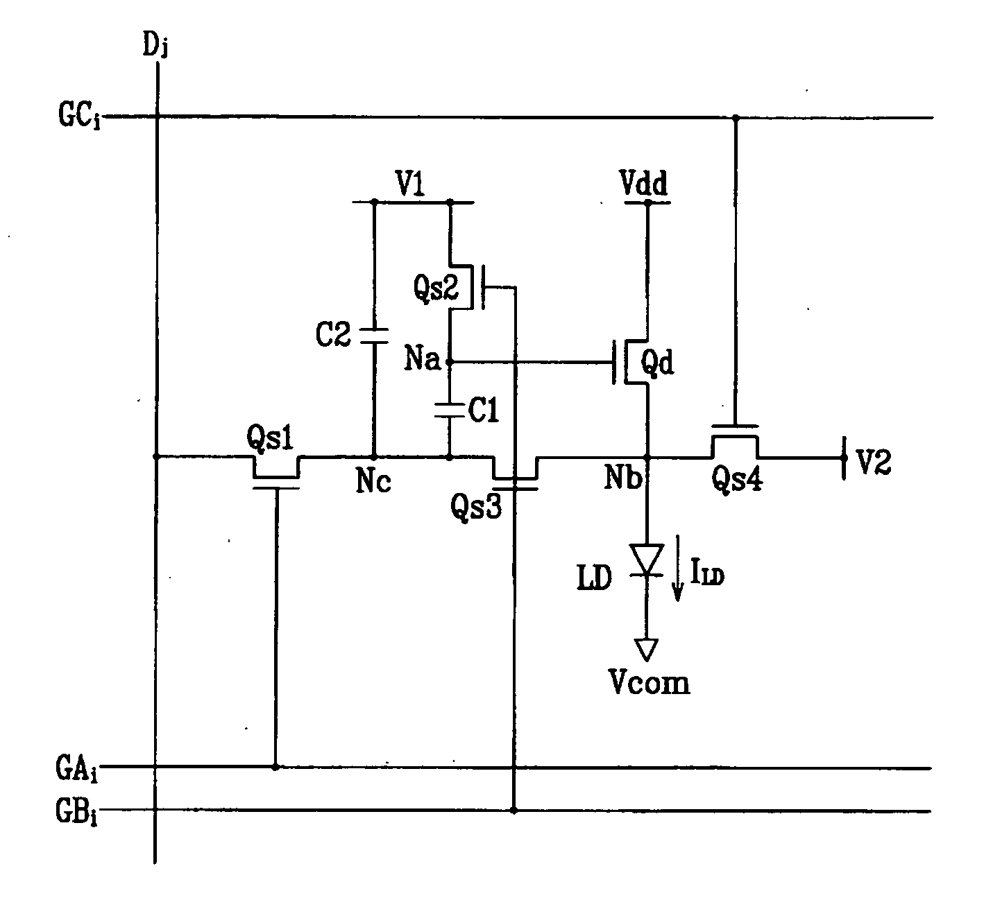
[0012] Embodiments of the present invention provide a display device capable of compensating the threshold voltage shift of the driving transistor and a driving method thereof to reduce image degradation.
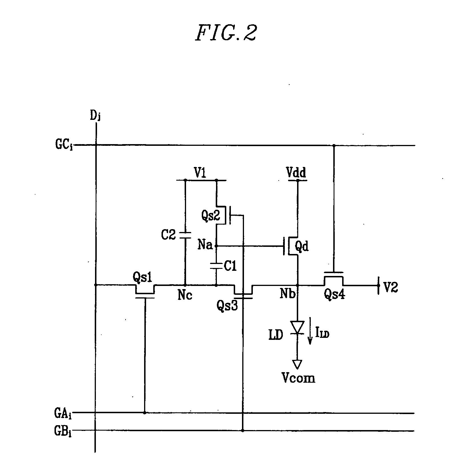
[0021] In an exemplary method of driving a display device with a driving transistor having a control terminal connected to a first node, an output terminal connected to a second node, an input terminal connected to a driving voltage, a light emitting element connected to the second node, and a capacitor connected between the first node and a third node, the method includes connecting a first voltage to the second node to prevent light emission of the light emitting element, connecting a second voltage larger than the first voltage to the first node, disconnecting the first voltage from the second node, disconnecting the second voltage form the first node, and connecting a data signal to the third node.

Problems solved by technology

A polysilicon transistor has several advantages, but it also has disadvantages such as the complexity of manufacturing polysilicon, thereby increasing the manufacturing cost.
In addition, it is difficult to make a wide screen OLED employing polysilicon transistors.
However, the threshold voltage (Vth) of the amorphous silicon transistor shifts over time, so that the current flowing in the light emitting element is non-uniform, resulting indegraded image quality.

Method used


Image

  • Display device and driving method thereof
  • Display device and driving method thereof
  • Display device and driving method thereof

Examples


Embodiment Construction

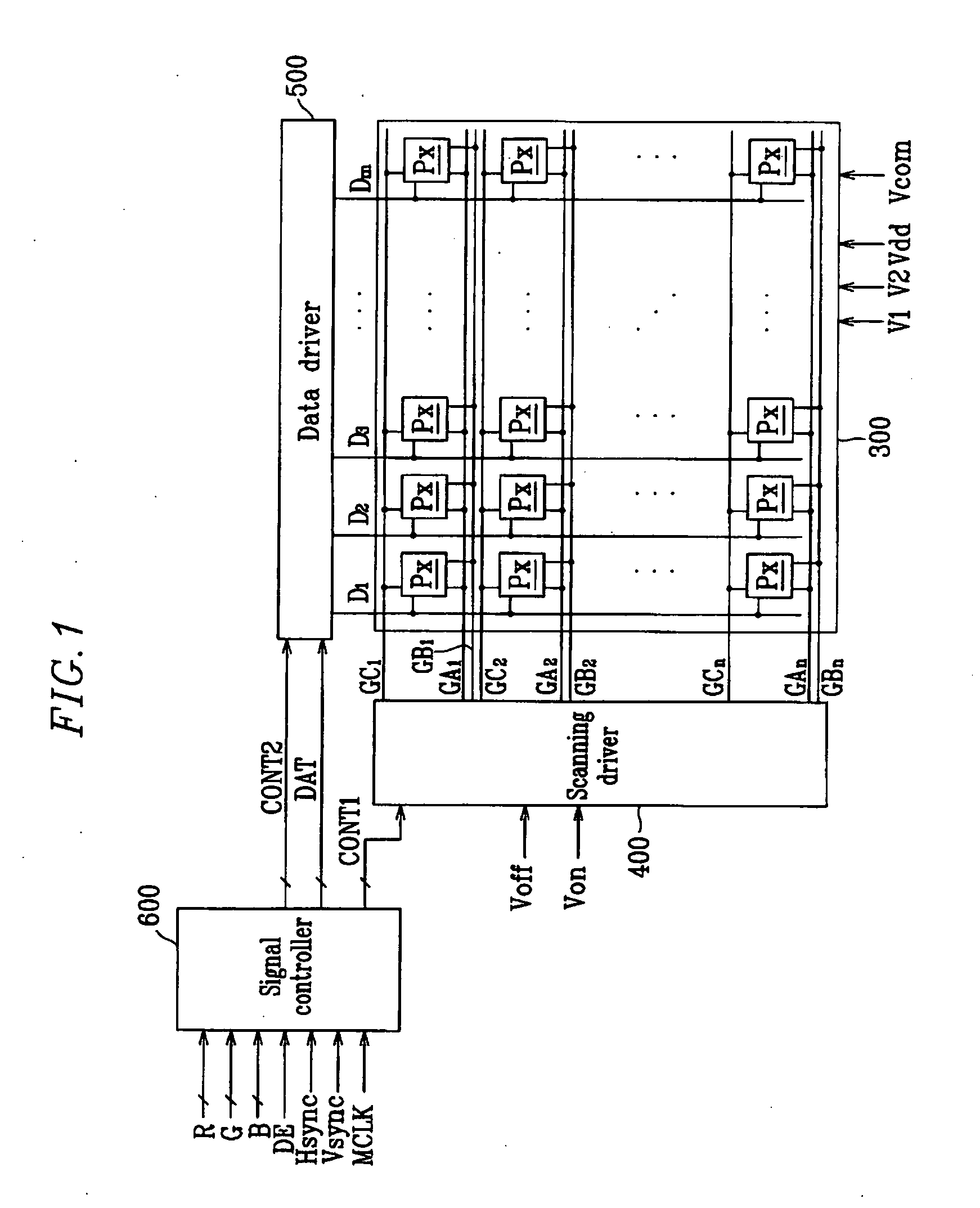
[0035]FIG. 1 is a block diagram of an OLED according to an embodiment of the present invention. The OLED includes a display panel 300, a scanning (i.e., gate) driver 400 and a data driver 500 connected to display panel 300, and a signal controller 600 connected to scanning driver 400 and data driver 500.

[0036] Display panel 300 includes first gate lines GA1-GAn, second gate lines GB1-GBn, third gate lines GC1-GCn, data lines D1-Dm, power supply lines (not shown), and a plurality of pixels Px. Gate lines carry gate signals and extend substantially parallel to one another, in a horizontal direction (in the example shown in FIG. 1), along rows of pixels. Data lines D1-Dm carry data signals and extend substantially parallel to one another in a vertical direction along columns of pixels. Power supply lines (not shown) carry a first voltage V1, a second voltage V2, and a driving voltage Vdd. In the embodiment illustrated in FIG. 1, pixels are arranged in a matrix configuration and are co...


PUM


Abstract

A display device includes a light emitting element connected to a common voltage, a driving transistor having a control terminal, an output terminal connected to the light emitting element, and an input terminal connected to a driving voltage, a first capacitor connected to the control terminal of the driving transistor, and a first switching transistor configured to transmit a data signal to the first capacitor. A first voltage is applied to the control terminal of the driving transistor, and a second voltage different from the first voltage and the driving voltage is applied to the output terminal of the driving transistor.

Description

CROSS-REFERENCE TO RELATED APPLICATION [0001] This application claims priority from Korean Patent Application No. 2005-0033149 filed on Apr. 21, 2005, the disclosure of which is hereby incorporated herein by reference in its entirety for all purposes. BACKGROUND [0002] 1. Field of the Invention [0003] The present invention relates generally to a display device, a driving method thereof, and in particular to an organic light emitting display (OLED) device and a driving method thereof. [0004] 2. Description of Related Art [0005] Many consumers want electronic devices with displays to be light and thin. Examples of such electronic devices include mobile communication systems, digital cameras, notebook PCs, monitors, and televisions. One method of reducing display size and weight is to use flat panel displays, such as organic light emitting displays (OLED). [0006] One type of flat panel display is an active matrix flat panel display. An active matrix flat panel display generally include...

Claims


Application Information

Patent Timeline
IPC IPC(8): G09G3/30H01L33/26H05B44/00
CPCG09G3/3233G09G3/3291G09G2300/043G09G2320/043G09G2300/0852G09G2310/0262G09G2300/0819A47J17/02B26D3/02B26D3/283B26D2003/288B26D2003/285
Inventor GOH, JOON-CHULCHOI, JOON-HOOCHOI, BEOHM-ROCK
Owner SAMSUNG ELECTRONICS CO LTD
Learn More