Organic el device and display

a technology of organic el and display screen, which is applied in the direction of discharge tube luminescent screen, discharge tube/lamp details, luminescent composition, etc., can solve the problems of insufficient luminance efficiency and half life inability to achieve color reproduction performance comparable with crt, and insufficient balance of organic el device. , to achieve the effect of good balance, good balance and stable emitted

Active Publication Date: 2006-10-26
JOLED INC
View PDF8 Cites 11 Cited by
  • Summary
  • Abstract
  • Description
  • Claims
  • Application Information

AI Technical Summary

Benefits of technology

[0007] In the organic EL device configured as above, holes (positive holes) injected from the anode is supplied into the light emitting layers from the red light emitting layer side. On the other hand, electrons injected from the cathode are supplied into the light emitting layers from the blue light emitting layer side. Therefore, the regions where the holes injected from the anode and the electrons injected from the cathode are coupled, i.e., light emission regions are respectively in the red, green, and blue light emitting layers, and each of the light-emitting layers emits light with the corresponding wavelength. Particularly, the lamination of the red light emitting layer, the green light emitting layer, and the blue light emitting layer in this order from the anode side permits a configuration such that the injection of holes and electrons as well as the light emission regions can be controlled and that the emission efficacy is higher and the half life of luminance is longer, as compared with the case where a blue light emitting layer, the green light emitting layer, and a red light emitting layer are laminated in this order from the hole transport layer side.
[0009] The hole transporting material included in the red light emitting layer as above may generally be a hole transporting material for constituting a hole transport layer provided between the anode and the light emitting-layers, and is preferably a red light emitting material having a hole transporting property (hole transporting red light emitting material). This enables a highly efficient and stable light emission with a high color purity. As the hole transporting red light emitting material, for example, a styrylarylene based material can be utilized. Particularly, the styrylarylene based materials described in Japanese Patent Laid-open Nos. 2001-110570 and 2002-226722 are preferably used. These materials are high in efficiency, have a long half life of luminance, and can be doped in a high density. Furthermore, since these materials have a hole transporting property, they make it possible to provide the red light emitting layer with an appropriate hole transporting property even where the host material of the red light emitting layer is an electron transporting material. Moreover, since the styrylarylene based material mentioned above can be doped with a dopant in a high concentration, the material can have a highest hole transporting property, so that where this material is used on the most anode side, holes can be securely supplied to the green light emitting layer provided on the cathode side.
[0010] Besides, in the organic-EL device as above, preferably, the green light emitting layer has a positive and negative charge transporting property for transporting both holes and electrons. This ensures that some of the holes injected through the red light emitting layer contribute to light emission in the green light emitting layer, and the rest of the holes are transported further into the blue light emitting layer disposed on the cathode side. Simultaneously, when electrons are injected through the blue light emitting layer on the cathode side, some of the electrons contribute to light emission in the green light emitting layer, and the rest of the electrons are transported into the red light emitting layer. With the green light emitting layer thus having the positive and negative charge transporting property, it is possible to obtain sufficient emission of light from each of the red, green and blue light emitting layers.
[0013] Particularly, the blue light emitting layer may have a configuration in which a positive and negative charge transporting blue light emitting layer and an electron transporting blue light emitting layer are laminated in this order from the anode side (from the green light emitting layer side). This ensures that the holes supplied via the green light emitting layer can be efficiently carried into a wide region in the blue light emitting layer, to permit highly efficient and stable light emission with high color purity.
[0017] According to such a display, by combining a plurality of the organic EL devices excellent in balance between the light emission colors with respective color filters, rays in the blue, green and red wavelength regions can be taken out in a good balance.
[0018] As has been described above, according to the organic EL device of the present invention, rays in the wavelength regions of three colors of red, green and blue can be stably emitted with a good balance and at a high efficiency for a long time. Therefore, by combining the organic EL devices with color filters, it is possible to configure a display excellent in color reproduction performance and capable of being driven for a long time.

Problems solved by technology

However, the white light emitting organic EL device with the above-mentioned configuration has the problem that the emission spectrum is largely varied with current and that the luminous efficacy and the half life of luminance are insufficient for display use.
In addition, the organic EL device is insufficient in balance of respective luminous intensities in blue, green and red wavelength regions.
Therefore, it has been impossible by use of such organic EL devices to obtain a display comparable in color reproduction performance with a CRT.

Method used


Image

  • Organic el device and display
  • Organic el device and display
  • Organic el device and display

Examples


example 1

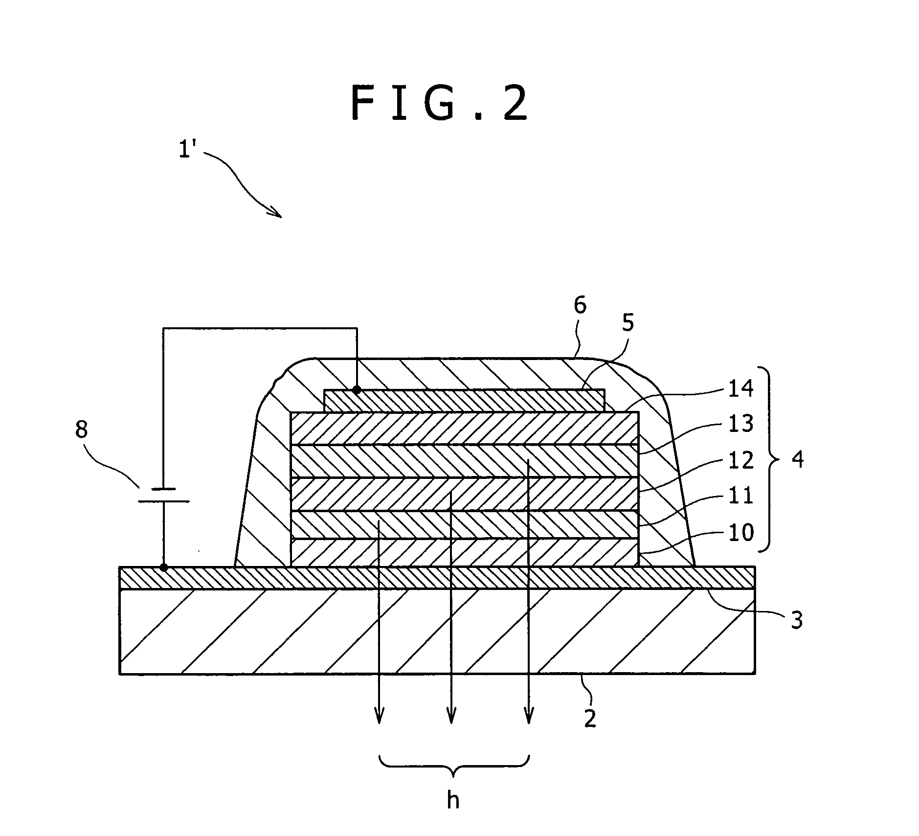
[0067] In Example 1, the bottom emission type organic EL device 1′ described referring to FIG. 2 was manufactured as follows.

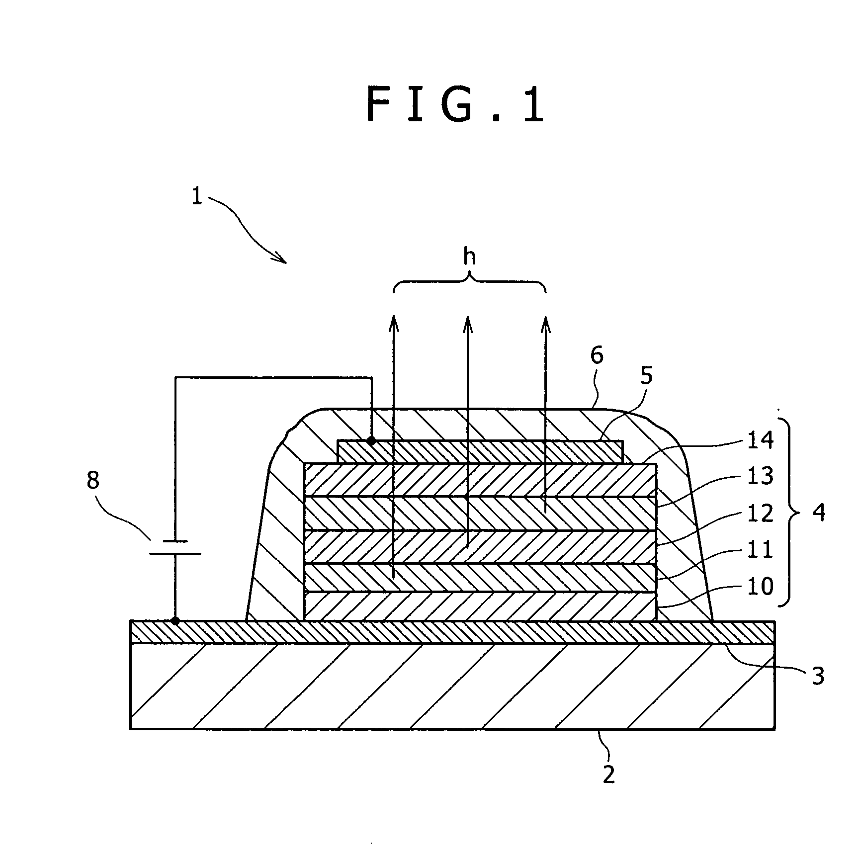
[0068] First, a cell for an organic EL device was produced in which a film of ITO (about 100 nm thick) as an anode 3 was formed on a substrate 2 composed of a 30 mm×30 mm glass plate, and other region than a central 2 mm×2 mm light emission region of the anode 3 was masked with an insulation film (omitted in the figure) by use of a photosensitive organic insulation material. Next, a metallic mask having an opening was disposed on the upper side of and in proximity to the substrate 2 in the condition where the opening was matched to the exposed portion of the anode 3 (ITO) to be each light emission region, and the following organic layers were sequentially formed by a vacuum evaporation method under a vacuum of 10−4 Pa or below.

[0069] First, as the hole transport layer 10, a film of m-MTDATA (4,4′,4″-tris(3-methylphenylphenylamino)-triphenylamine) represented...

example 2

[0079] In Example 2, an organic EL device 1′ was manufactured in the same manner as above, except that the blue light emitting layer 13 in Example 1 was replaced by a two-layer structure of a positive and negative charge transporting blue light emitting layer and an electron transporting light emitting layer which will be described below, for obtaining a good balance of white light emission.

[0080] In Example 2, the organic EL device 1′ was manufactured following the same procedure as that in Example 1, except that the blue light emitting layer 13 was formed by the following procedure. First, a co-deposition film composed of a mixture of DPVBi and α-NPD in a mixing ratio of 1:1 as a host doped with 3% of BCzVBi as a blue light emitting material was formed in a thickness of 10 nm. Thereafter, a co-deposition layer composed of DPVBi as a host doped with 3% of BCzVBi as a blue light emitting material was formed in a thickness of 20 nm, to obtain the blue light emitting layer 13 having ...


PUM

PropertyMeasurementUnit
thickaaaaaaaaaa
thickaaaaaaaaaa
thickaaaaaaaaaa

Abstract

An organic-EL device which has light emission components in three colors of red, green and blue in a good balance suited to use for a full-color display and which is capable of highly efficient and stable light emission for a long time. In the organic EL device (1) including an organic layer (4) having light emitting layers sandwiched between an anode (3) and a cathode (5), the light emitting layers include a red light emitting layer (11), a green light emitting layer (12), and a blue light emitting layer (13) laminated in this order from the side of the anode (3). The red light emitting layer (11) contains a hole transporting light emitting material and has a hole transporting property. In addition, the green light emitting layer has a positive and negative charge transporting property. Furthermore, the blue light emitting layer has an electron transporting property, and includes a positive and negative charge transporting blue light emitting layer and an electron transporting blue light emitting layer laminated in this order from the side of the anode (3).

Description

TECHNICAL FIELD [0001] The present invention relates to an organic EL device in which an organic layer including a plurality of light emitting layers is interposed between an anode and a cathode, and a display using the organic EL device. BACKGROUND ART [0002] In recent years, as a display to be used in place of a cathode ray tube (CRT), flat displays light in weight and low in power consumption have been an object of vigorous research and development. Among the flat displays, those displays which use self-light-emitting type display devices (so-called light emitting devices) such as organic EL (Electroluminescence) devices and organic EL devices have been paid attention to as a display capable of being driven with low power consumption. [0003] Configurations for achieving a full-color display mode with the display using the light emitting devices as above-mentioned include one in which an organic EL device capable of emitting white light is combined with color filters which respect...

Claims


Application Information

Patent Timeline
Patent Type & Authority Applications(United States)
IPC IPC(8): H01L51/50H05B33/14C09K11/06H05B33/12H01L51/00H05B33/22H05B33/26
CPCC09K11/06C09K2211/1007H01L51/005H01L51/0059H01L51/006H05B33/26H01L51/0071H01L51/0081H01L51/5036H05B33/14H01L51/0067H10K85/60H10K85/633H10K85/631H10K85/654H10K85/657H10K85/324H10K50/125H05B33/22
Inventor KASHIWABARA, MITSUHIROMATSUURA, RYOKO
Owner JOLED INC
Why Eureka
Try Eureka