Solid-state image sensing device
a solid-state image and sensing technology, applied in the direction of color television, television system, radio control device, etc., can solve the problems of poor light utilization efficiency and false color, and achieve the effect of high-quality image sensing and effective suppression of dark curren
- Summary
- Abstract
- Description
- Claims
- Application Information
AI Technical Summary
Benefits of technology
Problems solved by technology
Method used
Image

Examples
first embodiment
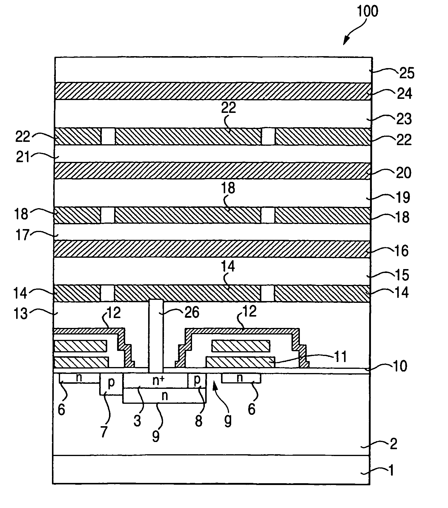
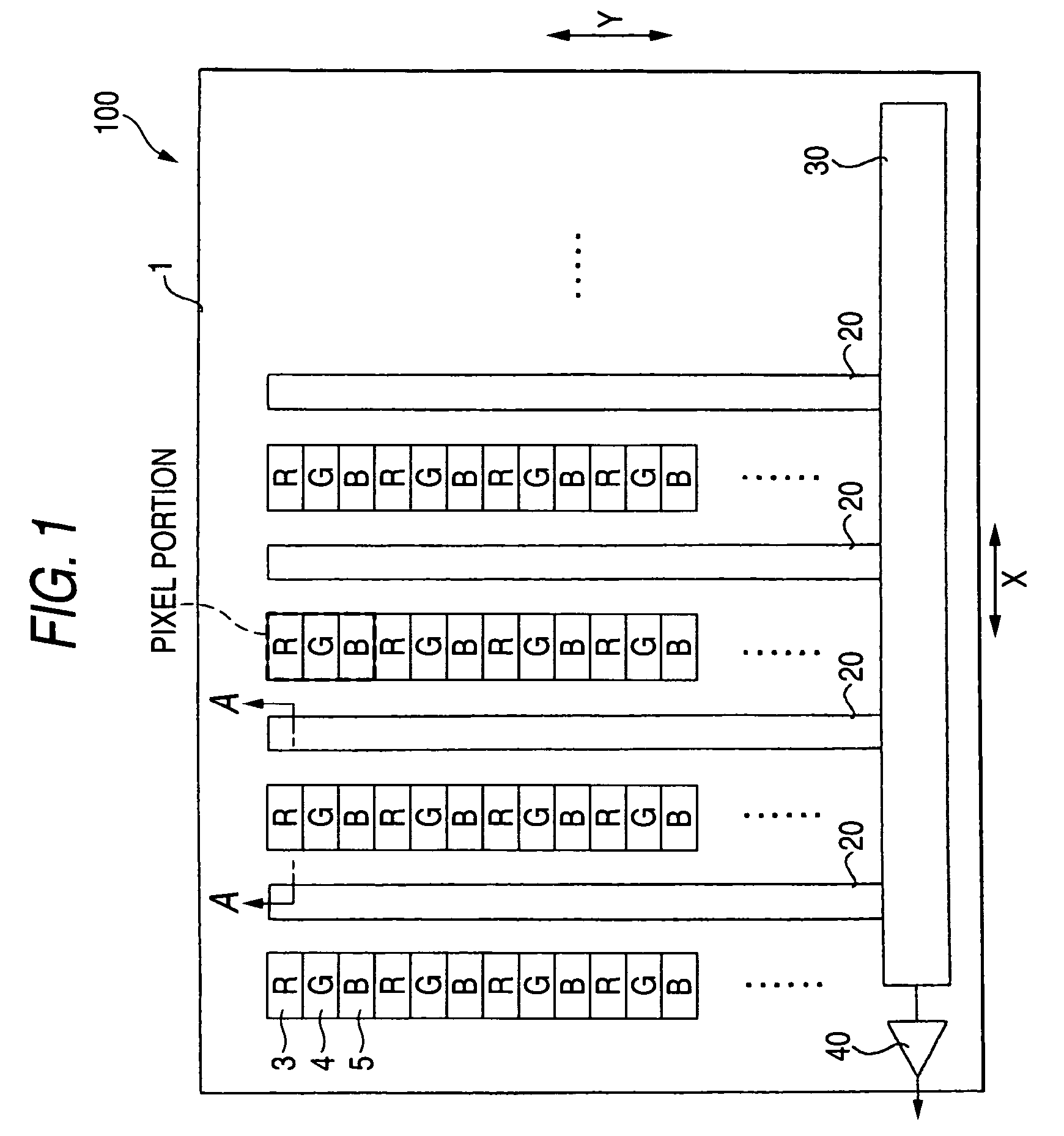
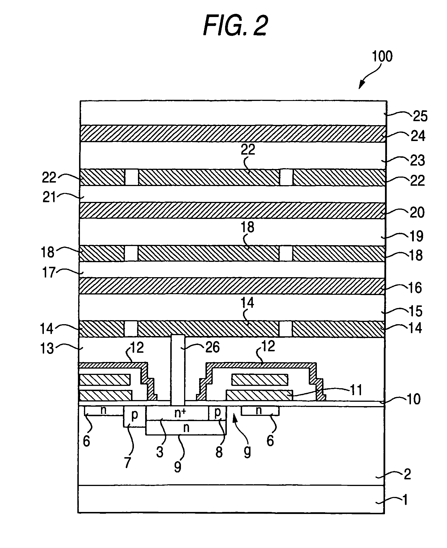
[0048]FIG. 1 is a typical plan view of a solid-state image sensing device for explaining a first embodiment of the invention. FIG. 2 is a typical sectional view taken along the line A-A, showing the solid-state image sensing device depicted in FIG. 1.
[0049] As shown in FIG. 2, an R photoelectric conversion film 15, a G photoelectric conversion film 19 and a B photoelectric conversion film 23 are stacked in this order above an n-type semiconductor substrate 1 of a first conduction type. The R photoelectric conversion film 15 detects red (R) light and generates red signal charge corresponding to the detected light. The G photoelectric conversion film 19 detects green (G) light and generates green signal charge corresponding to the detected light. The B photoelectric conversion film 23 detects blue (B) light and generates blue signal charge corresponding to the detected light. Incidentally, the order of stack of the respective photoelectric conversion films is not limited to this orde...
second embodiment
[0076]FIG. 8 is a partly sectional typical view of a solid-state image sensing device for explaining a second embodiment of the invention. In FIG. 8, the same constituent parts as those in FIG. 2 are referred to by the same numerals.
[0077] The solid-state image sensing device 200 shown in FIG. 8 is configured so that a p region 27 (fourth impurity region) which is a p-type impurity region lower in density than the p-well layer 2 is provided between the n+ region 3 and the n region 9 in addition to the solid-state image sensing device 100 shown in FIG. 2. The p region 27 needs to have a surface area at least equal to the surface area of the n+ region 3.
[0078]FIG. 9 is a view showing potential of the n+ region 3, the p region 27 and the n region 9 arranged in a depthwise direction perpendicular to the substrate in the partial section of the solid-state image sensing device shown in FIG. 8. As shown in FIG. 9, signal charge accumulated in the n+ region 3 and overflowing is poured int...
third embodiment
[0080] Although the first and second embodiments have been described on the case where a CCD type signal reading portion is used as the signal reading portion of the solid-state image sensing device, the same effect as in the first and second embodiments can be obtained also in the case where an MOS type signal reading portion is used as the signal reading portion of the solid-state image sensing device.
[0081]FIG. 10 is a partly sectional typical view of a solid-state image sensing device for explaining a third embodiment of the invention. In FIG. 10, the same constituent parts as those in FIG. 2 are referred to by the same numerals.
[0082] As shown in FIG. 10, the signal reading portion of the solid-state image sensing device 300 includes gate electrodes 31 and 32, an n region 6, an n region 33, and an amplification transistor 34.
[0083] The gate electrode 31 is equivalent to the transfer electrode 11 of the solid-state image sensing device 100. The gate electrode 31 is formed abo...
PUM
 Abstract
Description
Claims
Application Information
 - R&D
- Intellectual Property
- Life Sciences
- Materials
- Tech Scout
- Unparalleled Data Quality
- Higher Quality Content
- 60% Fewer Hallucinations
Browse by: Latest US Patents, China's latest patents, Technical Efficacy Thesaurus, Application Domain, Technology Topic, Popular Technical Reports.
© 2025 PatSnap. All rights reserved.Legal|Privacy policy|Modern Slavery Act Transparency Statement|Sitemap|About US| Contact US: help@patsnap.com