Amorphous layers in a magnetic tunnel junction device
a tunnel junction and amorphous layer technology, applied in the field of magnetic tunnel junction devices, can solve the problem of high positive magnetostriction of cofeb, and achieve the effect of improving sensitivity
- Summary
- Abstract
- Description
- Claims
- Application Information
AI Technical Summary
Benefits of technology
Problems solved by technology
Method used
Image
Examples
Embodiment Construction
[0016] It is known that the smoothness of TMR films, especially, the dielectric layer, is critical to achieving high dr / r and other vital parameters such as breakdown voltage(Vbd), the dropping rate of TMR versus applying voltage, and V50 (voltage at which dR / R is reduced by 50%). Thus improved techniques are needed to obtain a smooth film prior to depositing the dielectric layer.
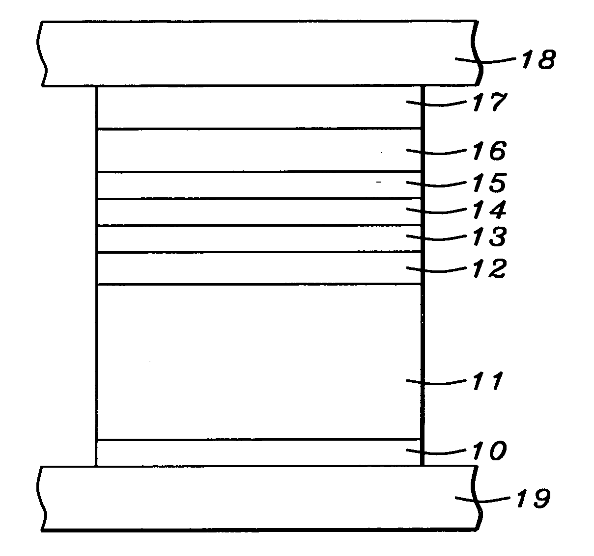
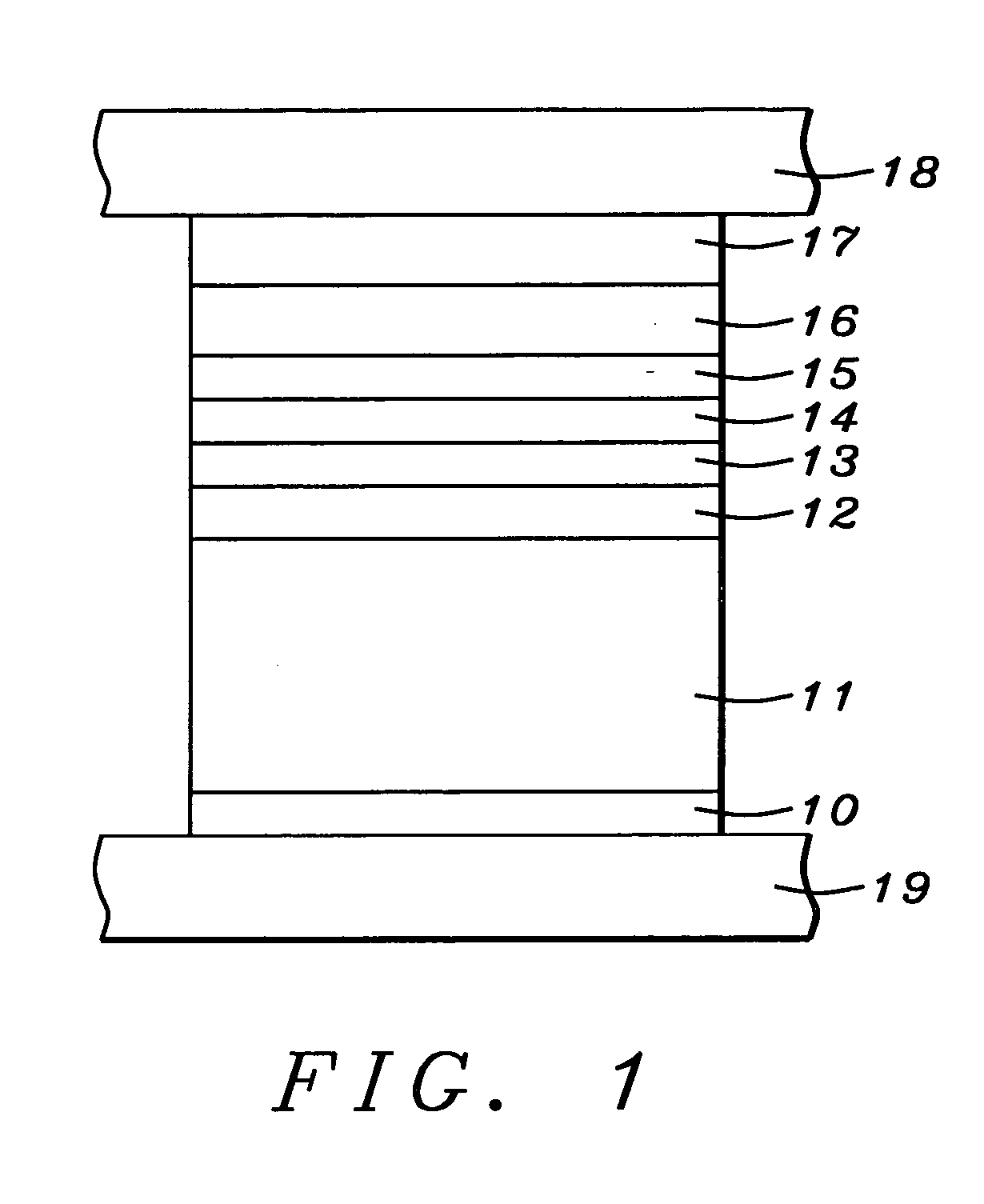
[0017] The structure of the invention is schematically illustrated in FIG. 1. Seen there are upper and lower conductive leads 18 and 19 with seed layer 10 being on layer 19. Antiferromagnetic layer 11 lies on seed layer 10 while AP2 and AP1 layers, 12 and 14 respectively, are immediately above it, with AFM decoupling layer 13 between them. Dielectric tunneling layer 15 lies on AP1 layer 14 and free layer 16 is on top of layer 15. Capping layer 17, on free layer 16, completes the structure.
[0018] To manufacture the invention, the layers are deposited in the order described in the previous paragraph and as ...
PUM
 Abstract
Description
Claims
Application Information
 - R&D
- Intellectual Property
- Life Sciences
- Materials
- Tech Scout
- Unparalleled Data Quality
- Higher Quality Content
- 60% Fewer Hallucinations
Browse by: Latest US Patents, China's latest patents, Technical Efficacy Thesaurus, Application Domain, Technology Topic, Popular Technical Reports.
© 2025 PatSnap. All rights reserved.Legal|Privacy policy|Modern Slavery Act Transparency Statement|Sitemap|About US| Contact US: help@patsnap.com


