
Inspection device for humidity sensor and method for adjusting sensor characteristics of humidity sensor

a technology of humidity sensor and inspection device, which is applied in the direction of measurement device, measurement device, instrument, etc., to achieve the effect of reducing the manufacturing cost of humidity sensor

Inactive Publication Date: 2006-09-14
DENSO CORP +1
View PDF6 Cites 9 Cited by
  • Summary
  • Abstract
  • Description
  • Claims
  • Application Information

AI Technical Summary

Benefits of technology

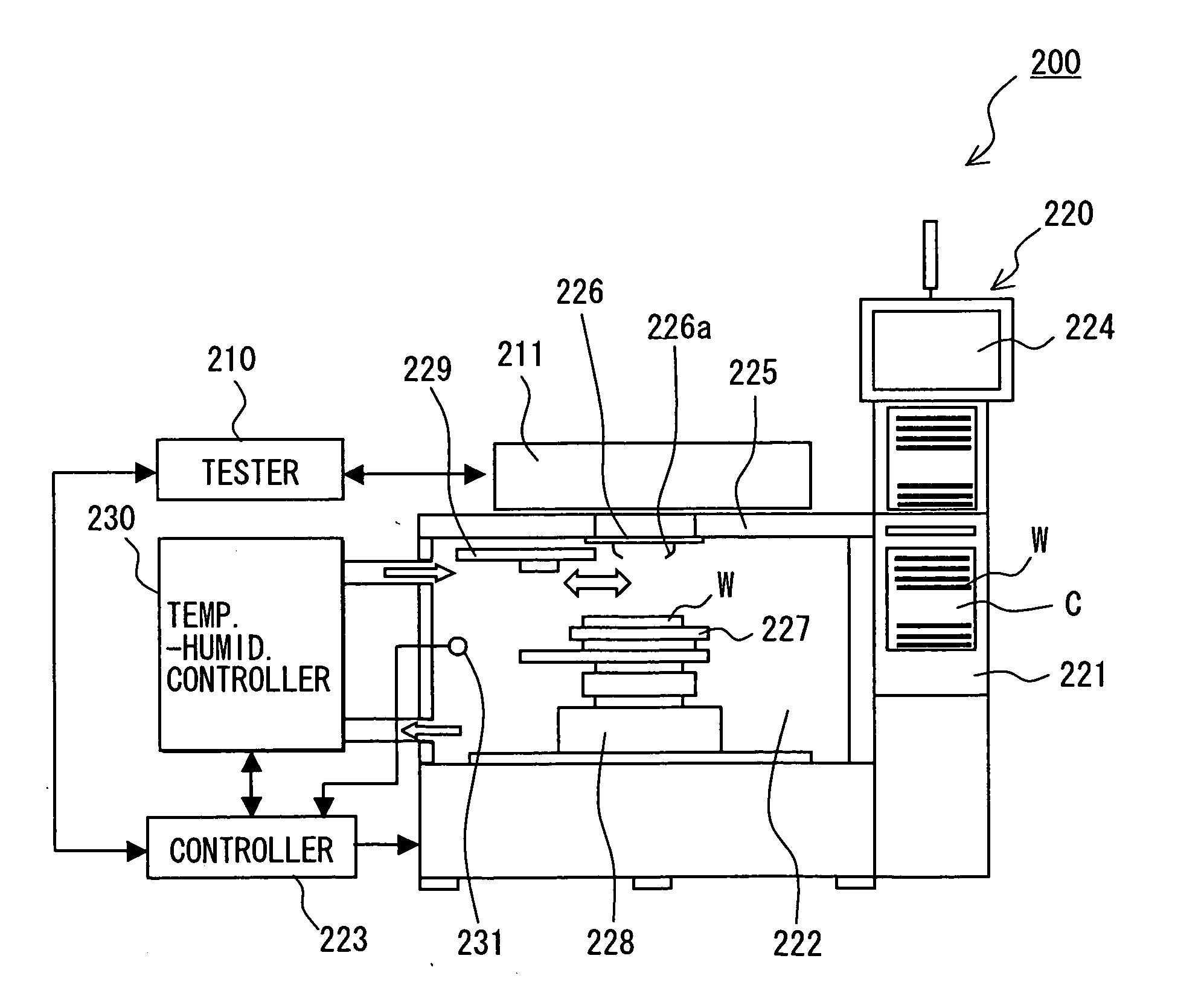
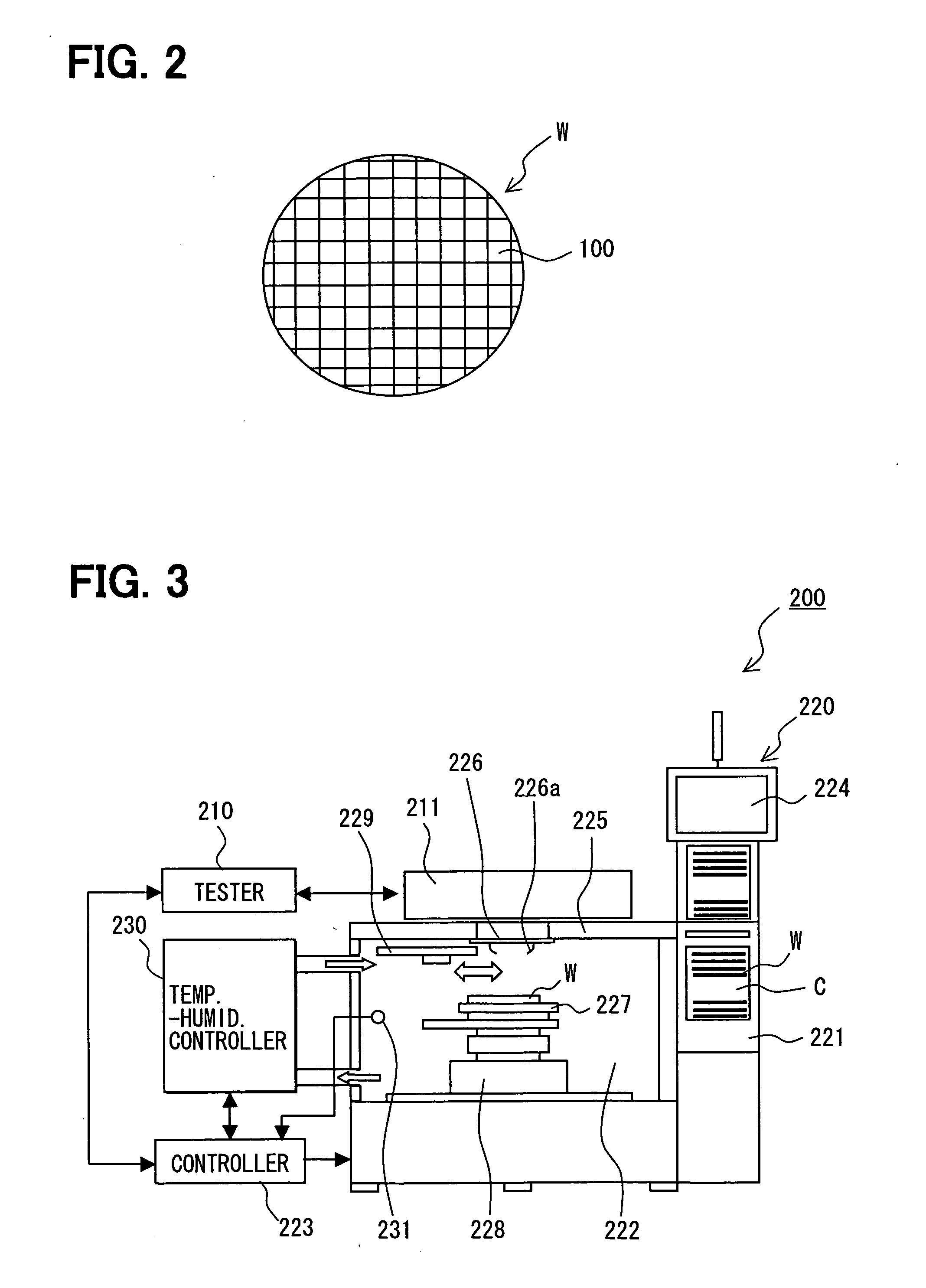
[0009] In the above inspection device, since the temperature-humidity control portion controls a temperature and a humidity in the inspection chamber to be a predetermined temperature-humidity condition, not only the probing test but also the sensor characteristic test are performed by the tester. Thus, the manufacturing cost of the humidity sensor is reduced. Further, by performing the sensor characteristic test and the probing test simultaneously, the manufacturing cost of the humidity sensor is much reduced.
[0011] In the above inspection device, the wafer is transported from one inspection chamber to another. Thus, the sensor characteristics of the humidity sensor are inspected effectively. Thus, the manufacturing cost of the humidity sensor is reduced. Further, since each inspection chamber is preliminarily controlled to have a predetermined temperature and a predetermined humidity, the waiting time for starting the test is shortened. Accordingly, many humidity sensors can be inspected within short time.
[0013] In the above method, not only the probing test but also the sensor characteristic test are performed even when the humidity sensor is in the wafer state, i.e., even when the wafer is not divided into multiple sensor chip. Further, on the basis of the test result, the sensor characteristics of the humidity sensor are adjusted. Thus, the manufacturing cost of the humidity senor is reduced.

Problems solved by technology

Even when the sensor portion and the circuit portion in the sensor are integrated into one IC chip, the inspection device disclosed in U.S. Pat. No. 6,037,793 cannot inspect the sensor characteristics of the sensor, which is in a wafer state before the sensor is divided from the wafer.

Method used


Image

  • Inspection device for humidity sensor and method for adjusting sensor characteristics of humidity sensor
  • Inspection device for humidity sensor and method for adjusting sensor characteristics of humidity sensor
  • Inspection device for humidity sensor and method for adjusting sensor characteristics of humidity sensor

Examples


first embodiment

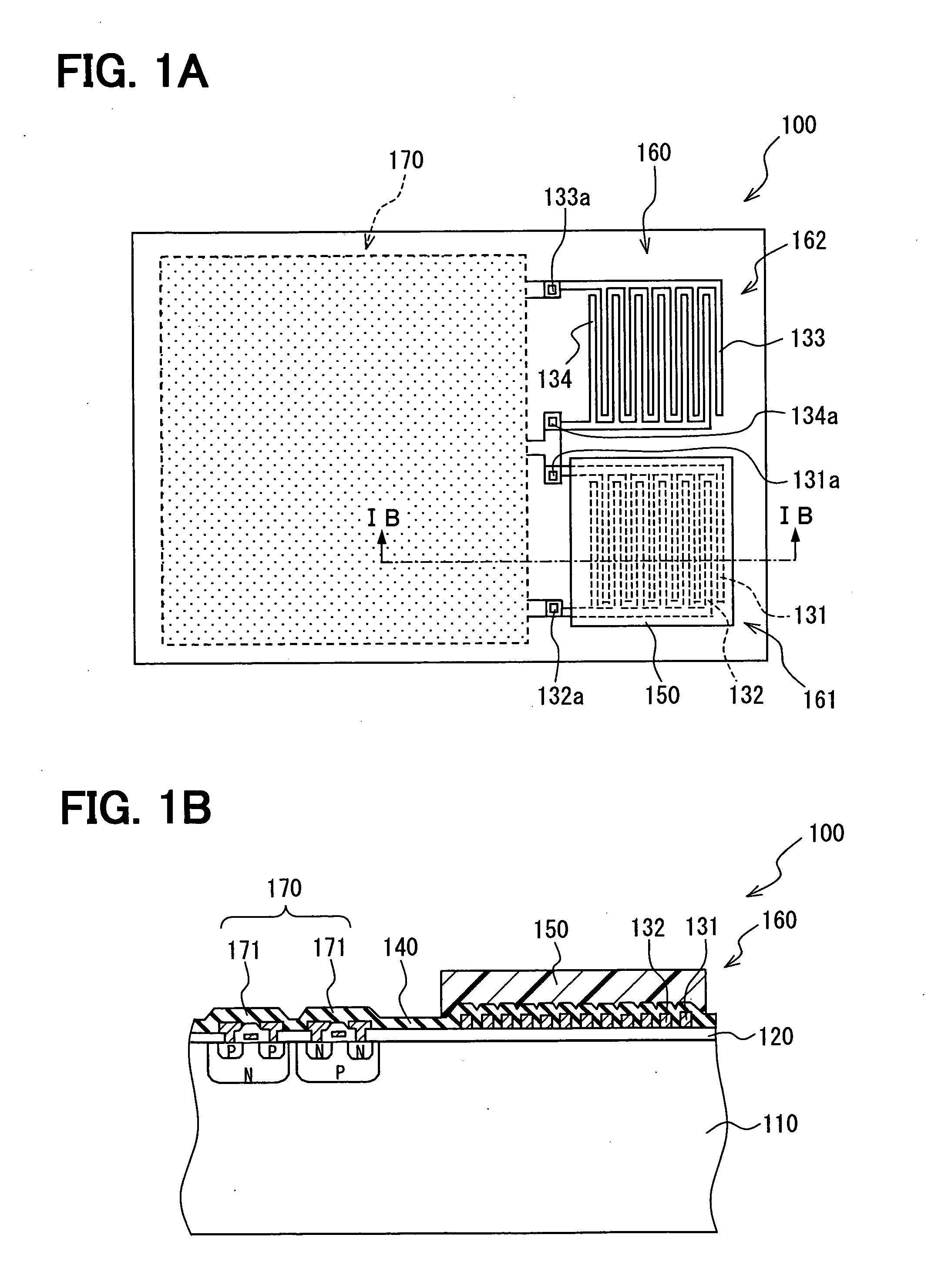
[0020] A humidity sensor 100 as an object of inspection of an inspection device according to a first embodiment of the present invention is shown in FIGS. 1A and 1B. The sensor 100 is formed to be one chip in a semiconductor wafer. In FIG. 1A, a circuit portion is omitted to show, and an electrode and a wiring are partially illustrated transparently.

[0021] It is required to decide whether an IC chip is a defective product and to select the IC chip as a non-defective product on the basis of a probing test as an electrical characteristic test before the wafer is divided into multiple IC chips. Specifically, the IC chip as a sensor chip in the wafer state is inspected by the inspection device whether electric parts such as a transistor and a resistor for composing the IC chip are normally formed without defect and whether the electric parts normally function as an electric circuit of the non-defective product.

[0022] When the IC chip is a sensor, it is required to perform a sensor cha...

second embodiment

[0051] An inspection device 200 according to a second embodiment of the present invention is shown in FIG. 4. FIG. 4 is a partially enlarged view showing the probe card 226 in the inspection device 200. The probe card 226 is fixed to a bottom side of a contact ring 232 by fixing means (not shown). The contact ring 232 and the probe card 226 are electrically connected with a spring pin 233. The contact ring 232 is also fixed to the head plate 225 with another fixing means (not shown).

[0052] The electric properties of the sensor 100 are detected and tested as follows. The tester head 211 press-contacts the top side of the contact ring 232 so that the tester head 211 and the contact ring 232 are electrically connected with the spring pin 233. Then, the main chuck 227 is elevated so that the probe 226a contacts the electrode pad of the humidity sensor 100 in the wafer W. Thus, the tester 210 inspects the electric properties of the sensor 100, i.e., the probing test. Specifically, the s...


PUM


Abstract

An inspection device inspects a humidity sensor having a sensor portion and a circuit portion, which are integrated into one chip. The inspection device includes: an inspection chamber for accommodating a wafer, in which a plurality of humidity sensors are disposed as a sensor chip in a wafer state; a probe for contacting an electrode pad of the circuit portion; a tester electrically connected to the probe for inspecting electric properties of the humidity sensor; and a temperature-humidity control portion for controlling a temperature and a humidity in the inspection chamber.

Description

CROSS REFERENCE TO RELATED APPLICATION [0001] This application is based on Japanese Patent Application No. 2005-64405 filed on Mar. 8, 2005, the disclosure of which is incorporated herein by reference. FIELD OF THE INVENTION [0002] The present invention relates to an inspection device for inspecting a humidity sensor in a wafer state and a method for adjusting the sensor characteristics of the humidity sensor in the wafer state. BACKGROUND OF THE INVENTION [0003] Conventionally, an inspection device for inspection sensor characteristics and electrical characteristics (electric properties) of an IC chip in the sensor is disclosed in, for example, U.S. Pat. No. 6,037,793. Here, the IC chip as a sensor chip is formed on a semiconductor wafer. [0004] The inspection device includes an inspection chamber (i.e., a probe chamber) for accommodating a semiconductor wafer, a probe (i.e., a probe of a probe card) as a contact member for contacting an electrode pad of the IC chip, and a tester f...

Claims


Application Information

Patent Timeline
IPC IPC(8): G01N35/00G01M99/00
CPCG01N27/223
Inventor ITAKURA, TOSHIKAZUISOGAI, TOSHIKI
Owner DENSO CORP
Learn More