Molded part and electronic device using the same

a technology of electronic devices and molded parts, which is applied in the direction of coupling device connections, other domestic articles, coatings, etc., can solve the problems of inability to establish the connection between the electrical connection terminal and the circuit board or the like having an electronic component mounted in the molded part by wire bonding, and the occurrence of shrinkage stress acting between the metallic section and the primary molding resin of the primary-molded article during secondary molding. , to achieve the effect of reducing the occurrence of shrink

Active Publication Date: 2006-08-24
HITACHI ASTEMO LTD
View PDF4 Cites 3 Cited by
  • Summary
  • Abstract
  • Description
  • Claims
  • Application Information

AI Technical Summary

Benefits of technology

[0015] One object of the present invention is to absorb and relieve the stress that the primary-molded article inserted into a molded part to be finally obtained suffers during resin shrinkage in multiple molding. More specifically, the invention is intended to provide an integrally multiple-molded part for electronic devices, capable of: preventing the occurrence of clearances between a bonding side face of an electrical connection terminal set and a molding resin in clearance-free contact with the bonding side face, by suppressing any actions of the stresses; obtaining stable frictional force at a contact region between a bonding surface of the electrical connection terminal set and an aluminum wire; thus obtaining the energy required for bonding; and ensuring high bondability.

Problems solved by technology

This may prevent sufficient frictional force from being generated on the bonding surface of each electrical connection terminal and on the contact region of the aluminum wire, with the result that the energy required for bonding may not be obtainable.
If these actually happen, the problem will occur in that connection between the electrical connection terminals and the circuit board or the like having an electronic component mounted in the molded part cannot be established by wire bonding.
Therefore, the suppression of the occurrence of the shrinkage stress acting between the metallic section and primary molding resin of the primary-molded article during secondary molding has been difficult.
As described above, however, since the metallic section molded by primary molding, such as a molded part for bonding, will have an exposed surface after secondary molding, it will be difficult to suppress the occurrence of shrinkage stresses during secondary molding.
As described above, however, since the metallic section molded by primary molding, such as a molded part for bonding, will have an exposed surface after secondary molding, it will be difficult to suppress the occurrence of a shrinkage stress during secondary molding.
The increases in the compactness and multifunctionality of connection terminals in recent years, however, have made it necessary to arrange a greater number of connection terminals, and this tendency, in turn, is reducing the terminals in width and in arrangement pitch.
Accordingly, the technique described in Patent Reference 3 is coming to pose at least two problems.
One is that a sufficient bonding space cannot be obtained at the terminal end portions to be resin-coated or at the terminal end portions to be provided with bends.
The other is that since the grooved or dimpled reverse side of the section to be bonded suffers significant plastic deformation, the surface to be bonded becomes prone to undulations, dents, or other defects, and deteriorates in quality.
For the connection terminals that were reduced in terminal width, therefore, there has been a limit to the effectiveness of the technique descried in Patent Reference 3.
In addition, since such a manufacturing method requires an application machine and curing equipment, there has been a problem in that costs are increased by a decrease in productivity.
Furthermore, the space required for the application of the epoxy material has been lost by the tendency towards reduced connection terminal areas due to the further compactness and multifunctionality of connection terminals in recent years, and the above method has also had its limits.

Method used


Image

  • Molded part and electronic device using the same
  • Molded part and electronic device using the same
  • Molded part and electronic device using the same

Examples


first embodiment

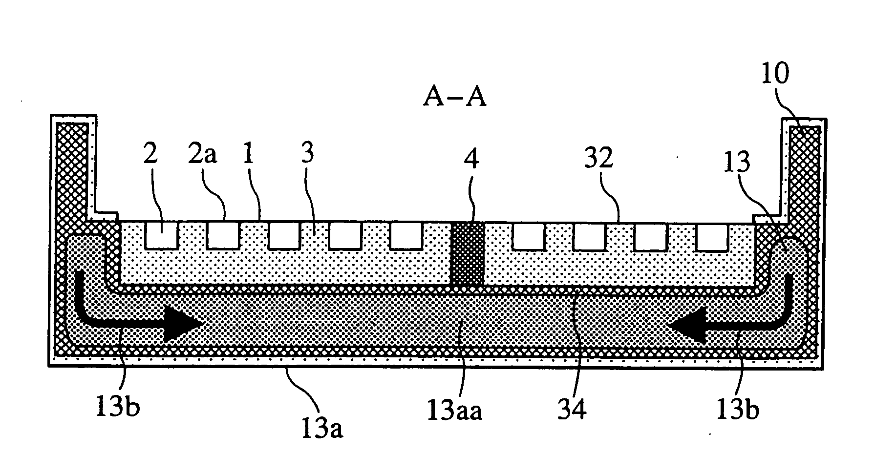
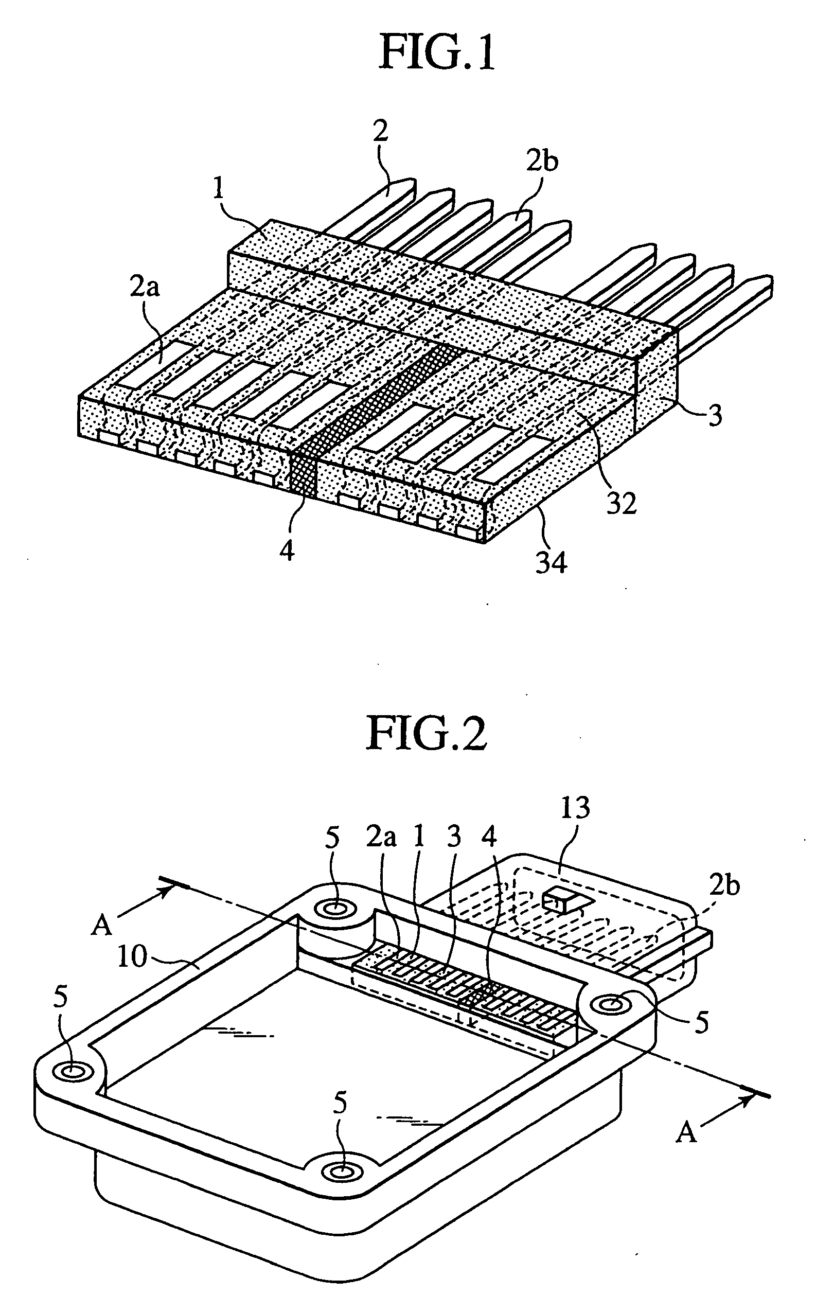
[0056] A first embodiment of an integrally multiple-molded part for electronic devices, based on the present invention, is shown in FIGS. 1 to 7, 13 and 14. This integrally multiple-molded part for electronic devices, based on the first embodiment, is formed by primary molding from resin a plurality of electrical connection terminals for electrical connection to outside and then forming, in a primary-molding resin section of the article formed by the primary-molding operation, a stress-absorbing structure made from a low-elasticity material softer than the primary molding resin, such as a stress-absorbing rubber material or elastomer material.

[0057]FIG. 1 is a perspective view of the primary-molded article after it has been formed in its primary-molding resin section by using a soft, low-elasticity material. FIG. 2 is a perspective view showing a main body of the integrally multiple-molded part for electronic devices, obtained after insert-molding of the primary-molded article show...

second embodiment

[0081] A second embodiment of an integrally multiple-molded part for electronic devices, based on the present invention, is shown in FIGS. 15 to 21. The same sections as those of the first embodiment are not described below.

[0082] In this second embodiment of an integrally multiple-molded part for electronic devices, a plurality of terminals for electrical connection to outside are an article formed by primary molding from resin. Also, a portion that has a small cross-sectional area in a primary-molding resin section of the primary-molded article and easily deforms is formed as a stress-absorbing structure in the primary-molding resin section of the primary-molded article, and more particularly, a recessed portion 52 is provided on the surface of a mold for primary molding.

[0083]FIG. 15 is a perspective view of the primary-molded article after a recessed portion has been formed in the primary-molding resin section of the primary-molded article. FIG. 16 is a perspective view showin...

third embodiment

[0099] A third embodiment of an integrally multiple-molded part for electronic devices, based on the present invention, is shown in FIGS. 22 to 24. The same sections as those of the foregoing embodiments are not described below.

[0100] In this third embodiment of an integrally multiple-molded part for electronic devices, as in the second embodiment, a plurality of terminals for electrical connection to outside are formed by primary molding from resin. Also, a portion that has a small cross-sectional area in a primary-molding resin section of the primary-molded article and easily deforms is formed as a stress-absorbing structure in the primary-molding resin section of the primary-molded article. In the present third embodiment, a recessed portion 54, in particular, is formed on a first surface 32 of primary molding resin 3.

[0101]FIG. 22 is a perspective view of the primary-molded article after a recessed portion has been formed in the primary-molding resin section of the primary-mol...


PUM

PropertyMeasurementUnit
stress-absorbingaaaaaaaaaa
bending rigidityaaaaaaaaaa
modulus of elasticityaaaaaaaaaa

Abstract

An integrally multiple-molded part for electronic devices is provided capable of absorbing and relieving the internal stresses of a multiple-molded part, preventing the occurrence of clearances between the bonding side face of each electrical connection terminal and a resin, obtaining stable frictional force at the contact region between the bonding surface of the electrical connection terminal and an aluminum wire, obtaining the energy required for bonding, and achieving high bondability. The surface of the molded electrical connection terminal section formed as a primary-molded article becomes exposed after secondary molding, and a stress-absorbing structure is formed in the primary molding resin section of the primary-molded article that serves as a transmission path for stresses associated with the resin shrinkage occurring when the secondary molding resin is cured.

Description

BACKGROUND OF THE INVENTION [0001] The present invention relates to molded parts for electronic devices, each obtained by inserting an insert article into a metallic mold and resin-molding the circumference of the insert article. More specifically, the invention relates to an integrally multiple-molded part for electronic devices, obtained by integrally insert-molding a plurality of electrical connection terminals a plurality of times. The invention is also directed to an electronic device that includes a circuit board with an electronic component mounted inside the integrally multiple-molded part for electronic devices. [0002] The increase in electronic control of devices in recent years has brought about the proliferation of the molded parts each obtained by insert-molding from resin a plurality of terminals for electrical connection to outside. In these molded parts, from the viewpoints of productivity and reliability, wire bonding is most commonly used to bond the electrical con...

Claims


Application Information

Patent Timeline
Patent Type & Authority Applications(United States)
IPC IPC(8): H01L23/02
CPCB29C37/005B29C45/14639B29C45/1671B29K2067/006B29K2709/08B29L2031/3061H01R13/405H01R43/24H01L2224/48091H01L2224/48247H01L2224/48472H01L2224/85181H01L2924/00014H01L2224/45124H01L2924/00
Inventor OOHASHI, KATSUHIDEAMAGI, SHIGEOMIYO, OSAMU
Owner HITACHI ASTEMO LTD
Why Eureka
Try Eureka