Organic electroluminescence device
a technology of electroluminescence device and electroluminescent device, which is applied in the direction of luminescent composition, thermoelectric device, chemistry apparatus and process, etc., can solve the problem of unpractically high driving voltage, and achieve the effect of long life and favorable light emission efficiency
- Summary
- Abstract
- Description
- Claims
- Application Information
AI Technical Summary
Benefits of technology
Problems solved by technology
Method used
Image
Examples
example 1
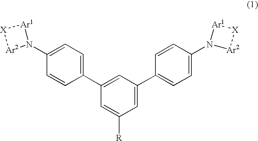
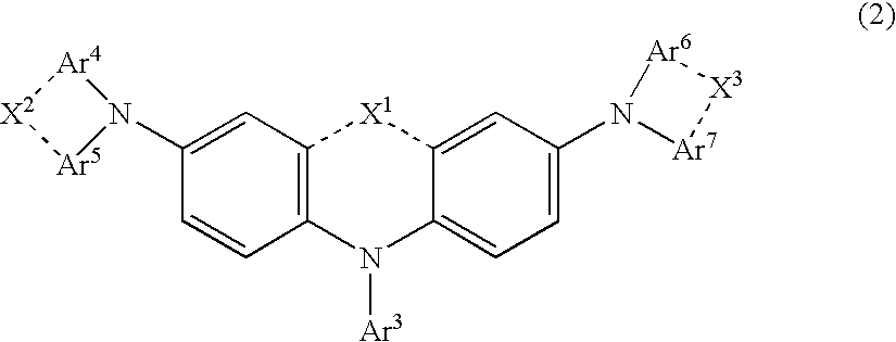
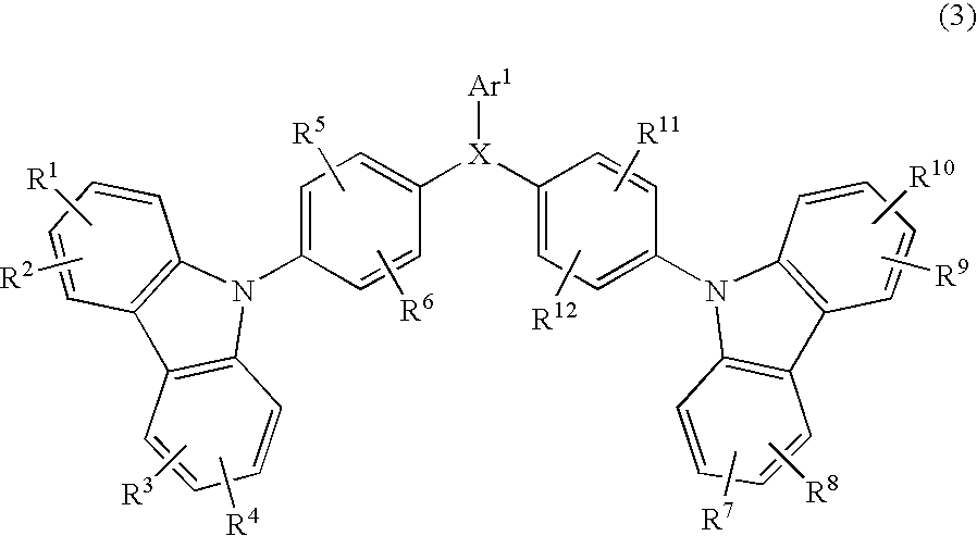
[0088] A glass substrate with an ITO transparent electrode having a size of 25 mm×75 mm and a thickness of 1.1 mm which was available from Geomatic Inc., was subjected to ultrasonic cleaning in isopropyl alcohol for 5 minutes, and then subjected to UV ozone cleaning for 30 minutes. The thus cleaned glass substrate with the transparent electrode was attached to a substrate holder of a vacuum deposition apparatus. First, a 10 nm-thick film made of copper phthalocyanine (hereinafter referred to merely as “CuPc film”) was formed on a surface of the substrate on which the transparent electrode was provided, so as to cover the transparent electrode. The thus formed CuPc film functioned as a hole injecting layer. Successively, a 30 nm-thick film made of the above TPAC as the hole transporting material was formed on the CuPc film. The thus formed TPAC film functioned as a hole transporting layer. Further, the below-mentioned compound PB102 as a host material was vapor-deposited on the TPAC ...
examples 2 to 5
[0090] The same procedure as in EXAMPLE 1 was repeated except for using as the hole transporting material, the respective compounds shown in Table 2 in place of TPAC, thereby producing an organic EL device. The thus produced organic EL device was subjected to measurements of light emission characteristics by the same method as in EXAMPLE 1. The results are shown in Table 2.
examples 8 to 10
[0100] The same procedure as in EXAMPLE 1 was repeated except for using as the host material of the light emitting layer, the following respective compounds shown in Table 4 in place of PB102, thereby producing an organic EL device. The thus produced organic EL device was subjected to measurements of light emission characteristics by the same method as in EXAMPLE 1. The results are shown in Table 4.
PUM
| Property | Measurement | Unit |
|---|---|---|
| triplet energy | aaaaa | aaaaa |
| ionization potential | aaaaa | aaaaa |
| triplet energy | aaaaa | aaaaa |
Abstract
Description
Claims
Application Information
 - R&D
- Intellectual Property
- Life Sciences
- Materials
- Tech Scout
- Unparalleled Data Quality
- Higher Quality Content
- 60% Fewer Hallucinations
Browse by: Latest US Patents, China's latest patents, Technical Efficacy Thesaurus, Application Domain, Technology Topic, Popular Technical Reports.
© 2025 PatSnap. All rights reserved.Legal|Privacy policy|Modern Slavery Act Transparency Statement|Sitemap|About US| Contact US: help@patsnap.com


