


Quick Research
Generate reliable direction feasibility study reports for your R&D in just a few steps.

Technical Q&A
Discover and master advanced knowledge NOW. Basics, ideas, possibilities, all at once.

Find Solutions
As an expert in R&D theories, this can generate solutions to your technical problems instantly.

Evaluate Feasibility
Analyze your overall solution with one click, know your potential R&D risks in advance.

Monitor Landscape
Get weekly tech updates, stay abreast of the latest tech innovations and key insights.
Method of forming film pattern, device, method of manufacturing device, electro-optical device, and electronic apparatus
- Summary
- Abstract
- Description
- Claims
- Application Information
AI Technical Summary
Benefits of technology
Problems solved by technology
Method used
Image

Examples
first embodiment
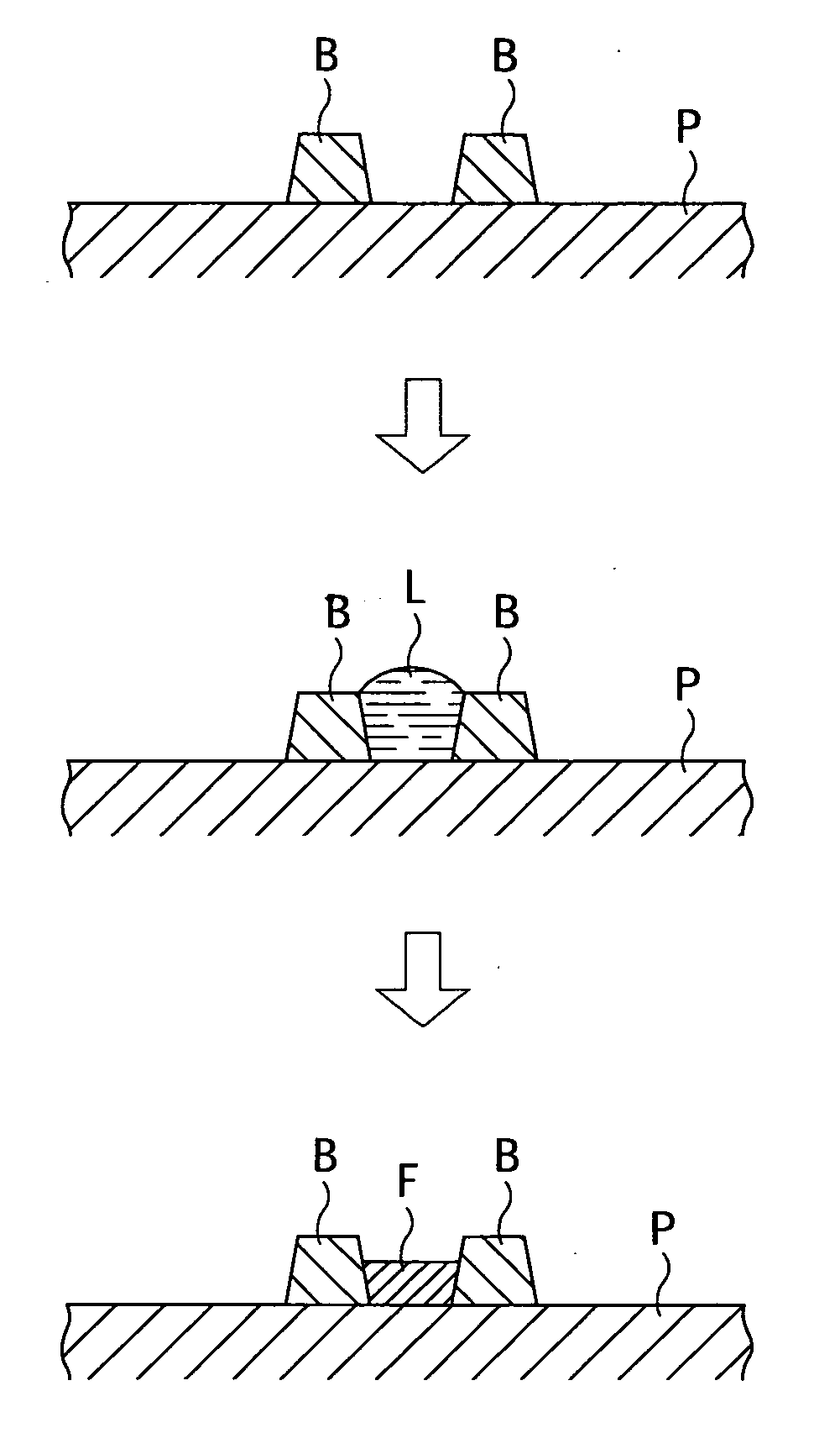
[0092] Next, a method of forming a wiring pattern according to a first embodiment of the invention will be described with reference to FIGS. 4, 5A to 5E, 6A to 6E, and 7A to 7D. FIG. 4 is a flow chart illustrating an example of a method of forming a film pattern according to the present embodiment, and FIGS. 5A to 5E, 6A to 6E, and 7A to 7D are schematic views showing an order of forming a film pattern.
[0093] As shown in FIG. 4, in a method of forming a wiring pattern according to the present embodiment, the above-described ink for formation of wiring pattern is disposed on a substrate and a conductive wiring pattern is formed on the substrate. Specifically, the method generally includes a lyophilic treatment process S1 for performing lyophilic treatment on a surface of the substrate, bank forming processes S2 to S6 for forming banks according to the wiring pattern on the lyophilic substrate, a residue removing process S7 for removing residue between banks, a lyophobic treatment pr...
second embodiment
[0122] Next, a method of forming a film pattern according to a second embodiment of the invention will be described with reference to the flow chart of FIGS. 4, 8A to 8D, and 9A to 9D. In the embodiment, the same members or portions as in the first embodiment are denoted by the same reference numerals, and detailed explanation thereof will be omitted. In addition, in FIGS. 8A to 8D and 9A to 9D, processes subsequent to a material disposition process will be omitted.
[0123] While the bank material in the first embodiment includes the material containing polysilazane as the main component and photosensitive polysilazane containing photoacid generator, the bank material in the second embodiment includes a material using polysiloxane as the main component and photosensitive polysiloxane containing photoacid generator.
[0124] The second embodiment is similar to the first embodiment except that the former has no humidification treatment in the developing and bank baking processes S4 and S...
third embodiment
[0130] Next, a method of forming a film pattern according to a third embodiment of the invention will be described with reference to FIGS. 10, 11A to 11E, and 12A to 12E. FIG. 10 is a flow chart illustrating an example of a method of forming a wiring pattern according to the third embodiment, and FIGS. 11A to 11E and 12A to 12E are views schematically illustrating the order of forming the wiring pattern. The third embodiment is similar to the first embodiment except that the lyophobic treatment is performed before the development treatment. Therefore, the same members or portions as in the first embodiments are denoted by the same reference numerals, and the same processes will not be explained. Processes subsequent to a material disposition process will be omitted in FIGS. 11A to 11E and 12A to 12E.
[0131] In the embodiment, the processes S11 to S13 shown in FIGS. 11A to 11D are the same as the processes S1 to S3 shown in FIGS. 5A to 5D in the first embodiment. In the first embodim...
PUM
 Abstract
Description
Claims
Application Information
 - R&D Engineer
- R&D Manager
- IP Professional
- Industry Leading Data Capabilities
- Powerful AI technology
- Patent DNA Extraction
Browse by: Latest US Patents, China's latest patents, Technical Efficacy Thesaurus, Application Domain, Technology Topic, Popular Technical Reports.
© 2024 PatSnap. All rights reserved.Legal|Privacy policy|Modern Slavery Act Transparency Statement|Sitemap|About US| Contact US: help@patsnap.com