Ultraviolet light transparent nanoparticles for photoresists

Inactive Publication Date: 2006-07-27
INTEL CORP
View PDF4 Cites 25 Cited by
  • Summary
  • Abstract
  • Description
  • Claims
  • Application Information

AI Technical Summary

Problems solved by technology

This results in uneven patterning of the photoresist, where the portions of the photoresist that are nearer to the top are over-exposed and the portions of the photoresist near the bottom are incompletely exposed.
But, the boron from the photoresists may poison the underlying semiconductor based devices because boron is a dopant.
Additionally, the reduction of the amount of oxygen in photoresists increases the hydrophobic properties of the photoresist that may lead to adhesion and wetting problems, and ultimately increased defectivity due to these problems.
But, the formation of the skin to reduce the impact of the photoresist's absorption of the ultraviolet light also reduces photospeed and resolution of the photoresist.

Method used


Image

  • Ultraviolet light transparent nanoparticles for photoresists
  • Ultraviolet light transparent nanoparticles for photoresists
  • Ultraviolet light transparent nanoparticles for photoresists

Examples


Embodiment Construction

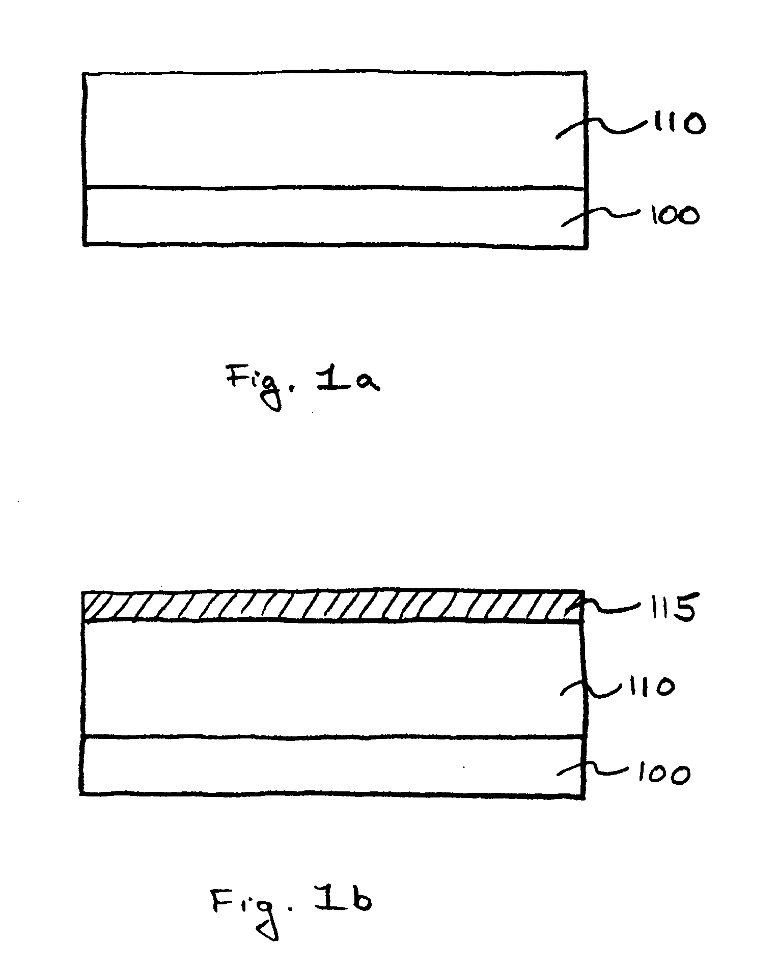
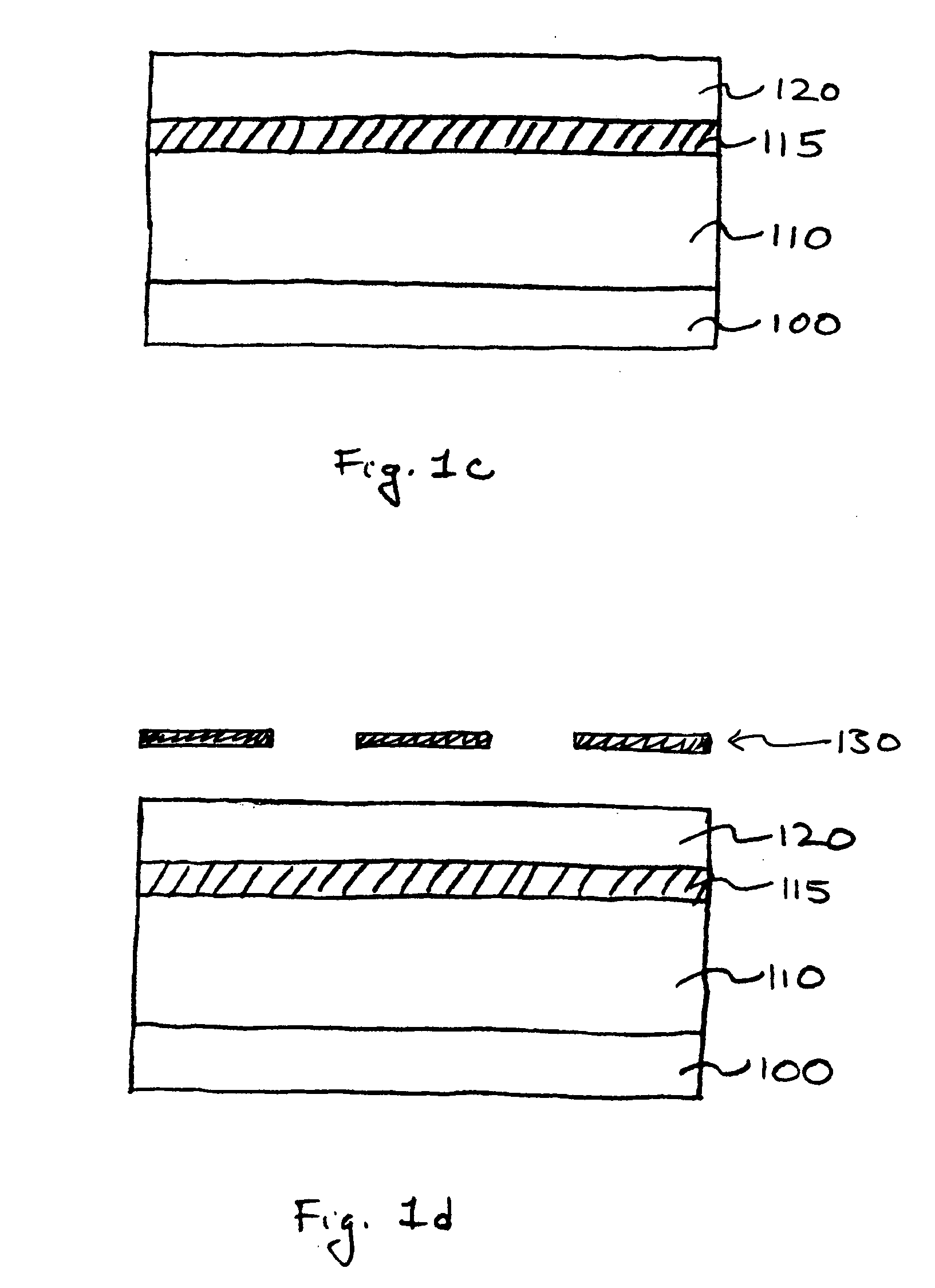
[0009] Described herein are photoresist formulations including ultraviolet light transparent nanoparticles and methods of using the photoresists. In the following description numerous specific details are set forth. One of ordinary skill in the art, however, will appreciate that these specific details are not necessary to practice embodiments of the invention. While certain exemplary embodiments of the invention are described and shown in the accompanying drawings, it is to be understood that such embodiments are merely illustrative and not restrictive of the current invention, and that this invention is not restricted to the specific constructions and arrangements shown and described because modifications may occur to those ordinarily skilled in the art. In other instances, well known semiconductor fabrication processes, techniques, materials, equipment, etc., have not been set forth in particular detail in order to not unnecessarily obscure embodiments of the present invention.

[0...


PUM


Abstract

The transparency of photoresist films to ultraviolet light may be increased without sacrificing photospeed or resolution of the photoresist by including ultraviolet light transparent nanoparticles to the photoresist formulations. The ultraviolet light transparent nanoparticles may be included in the photoresist formulations as filler to “dilute” the ultraviolet light opacity of the photoresist, as side-chains to the photoimageable species that form the photoresist matrix, or as the photoimageable species themselves that form the backbone of the photoresist matrix. The photoresist formulation may also be a hybrid solution of any of these variations on the inclusion of the ultraviolet light transparent nanoparticles. The ultraviolet light transparent nanoparticles may mostly contain carbon or silicon.

Description

BACKGROUND OF THE INVENTION [0001] 1. Field of the Invention [0002] The present invention relates to the field of photolithography to form integrated circuits and more particularly to the field of photoresists used in photolithography. [0003] 2. Discussion of Related Art [0004] Photolithography is used in the field of integrated circuit processing to form the patterns that will make up the features of an integrated circuit. A photoresist is employed as a sacrificial layer to transfer a pattern to the underlying substrate. This pattern may be used as a template for etching or implanting the substrate. Patterns are typically created in the photoresist by exposing the photoresist to radiation through a mask. The radiation may be ultraviolet light, extreme ultraviolet (EUV) light, or an electron beam. In the case of a “direct write” electron beam, a mask is not necessary because the features may be drawn directly into the photoresist. Most photolithography is done using either the “i-li...

Claims


Application Information

Patent Timeline
IPC IPC(8): G03C1/76
CPCG03F7/0047G03F7/0382G03F7/0392
Inventor MEAGLEY, ROBERT P.
Owner INTEL CORP
Why Eureka
Try Eureka