Method for forming high-K charge storage device
a memory device and high-k charge technology, applied in semiconductor/solid-state device manufacturing, basic electric elements, electric devices, etc., can solve the problems of scaling and scaling issue, and achieve the effect of reducing repetition
- Summary
- Abstract
- Description
- Claims
- Application Information
AI Technical Summary
Benefits of technology
Problems solved by technology
Method used
Image
Examples
first example embodiment
II. FIRST EXAMPLE EMBODIMENT
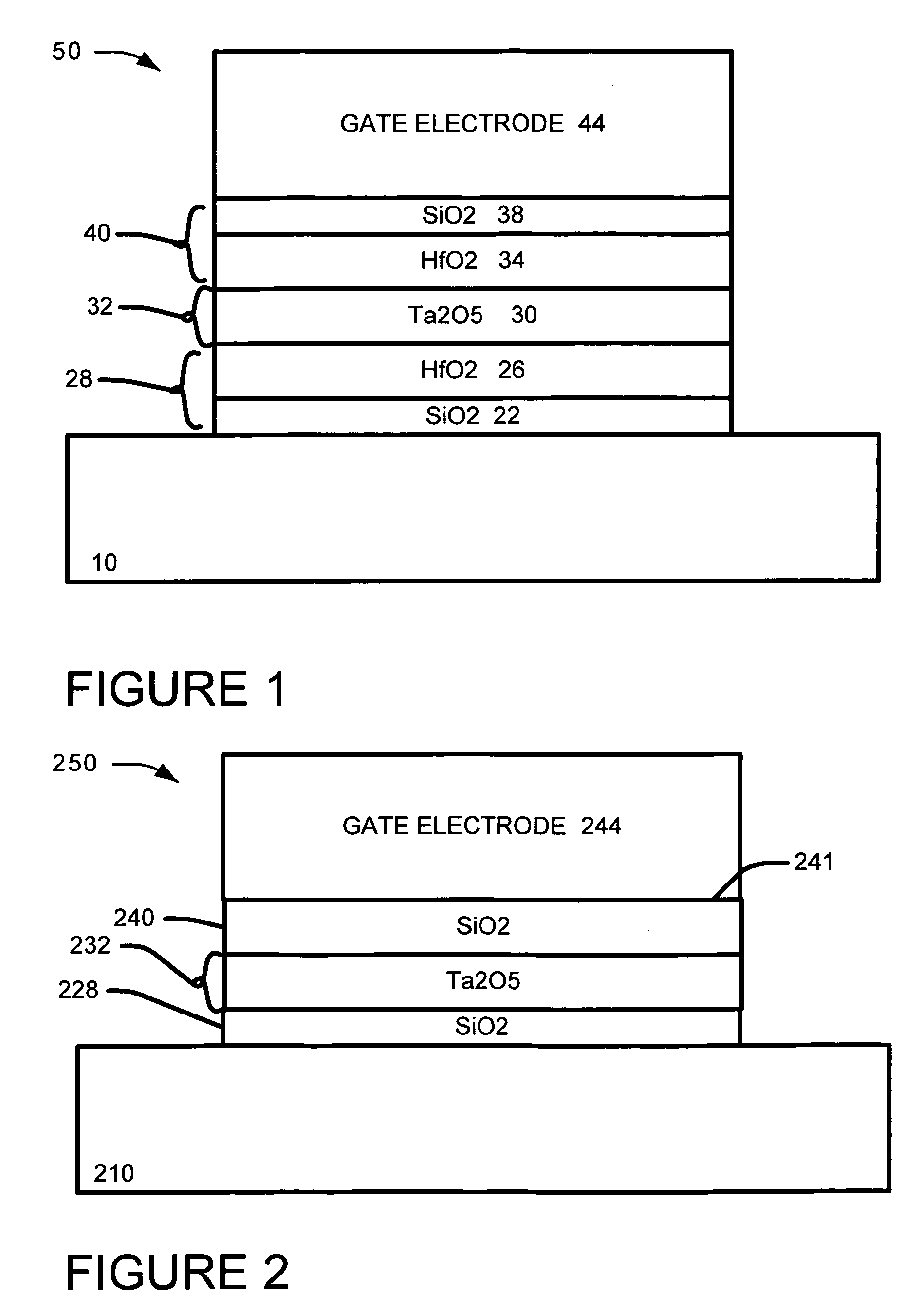
[0057] The first example embodiment of a memory structure is depicted in FIG. 1. It preferably employs a top blocking layer 40 comprised of SiO2 / HfO2 3834, a charge storage layer 32 comprised of Ta2O5, and a bottom tunnel dielectric 28 comprised of HfO2 / SiO22622. The top and bottom SiO2 3822 are preferably very thin, 2 layers serves to improve the retention and interfacial quality for the bottom Si and gate electrode. The HfO2 layers can improve the erase speed as compared to a conventional SONOS. The top HfO2 layer 34 thickness preferably ranges from 5 to 20 nm, while the bottom HfO2 layer 26 thickness preferably ranges from 1 to 6 nm. The Ta2O5 layer 30 preferably thickness ranges from 3 to 8 nm. Using high-k materials allow further device and voltage scaling. They can be deposited using CVD or PVD processes. The gate electrode 44 can be metal or polysilicon.
[0058] A first example embodiment for a method of fabrication of a floating gate non-volatile m...
second example embodiment
III. SECOND EXAMPLE EMBODIMENT
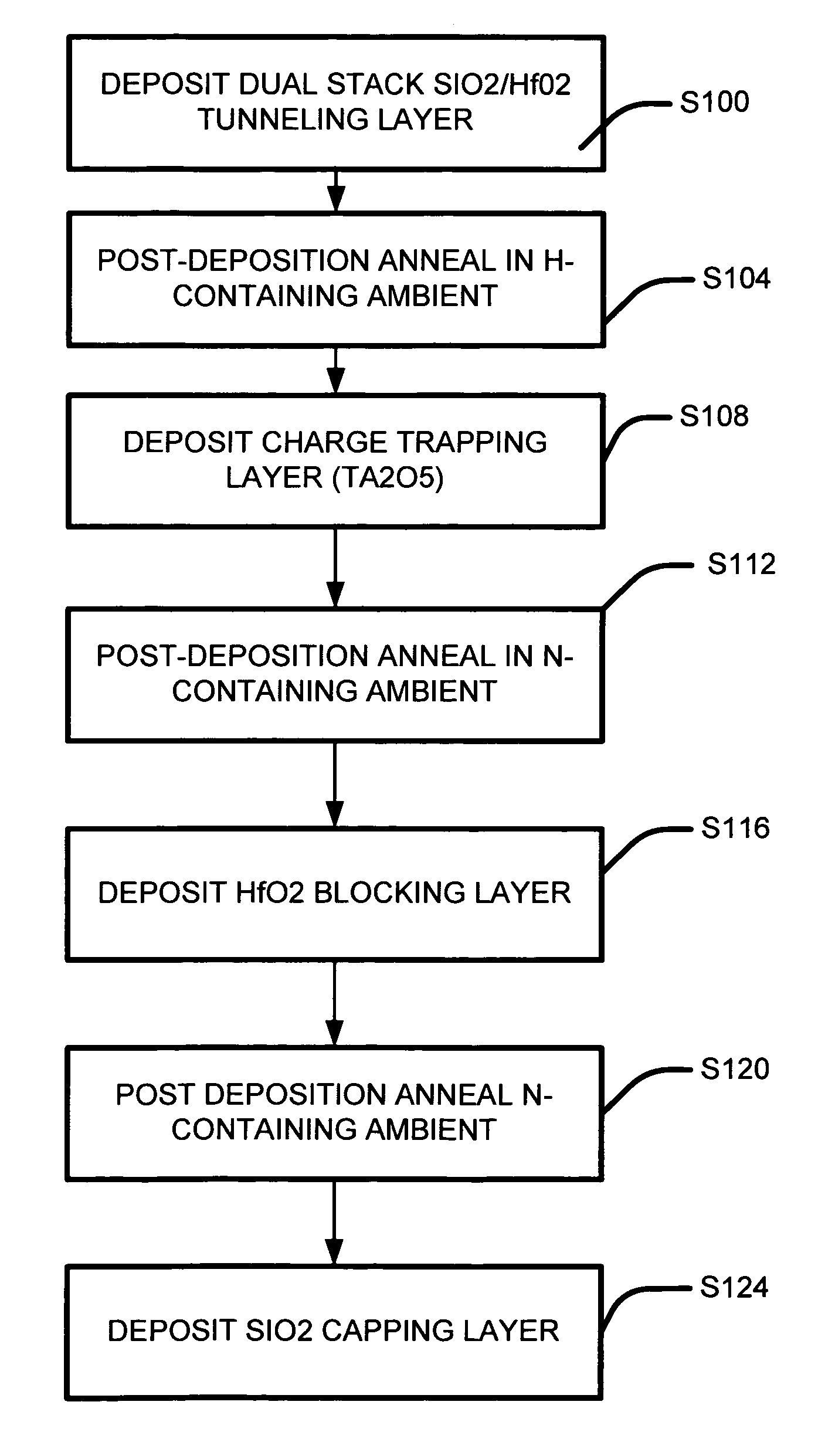
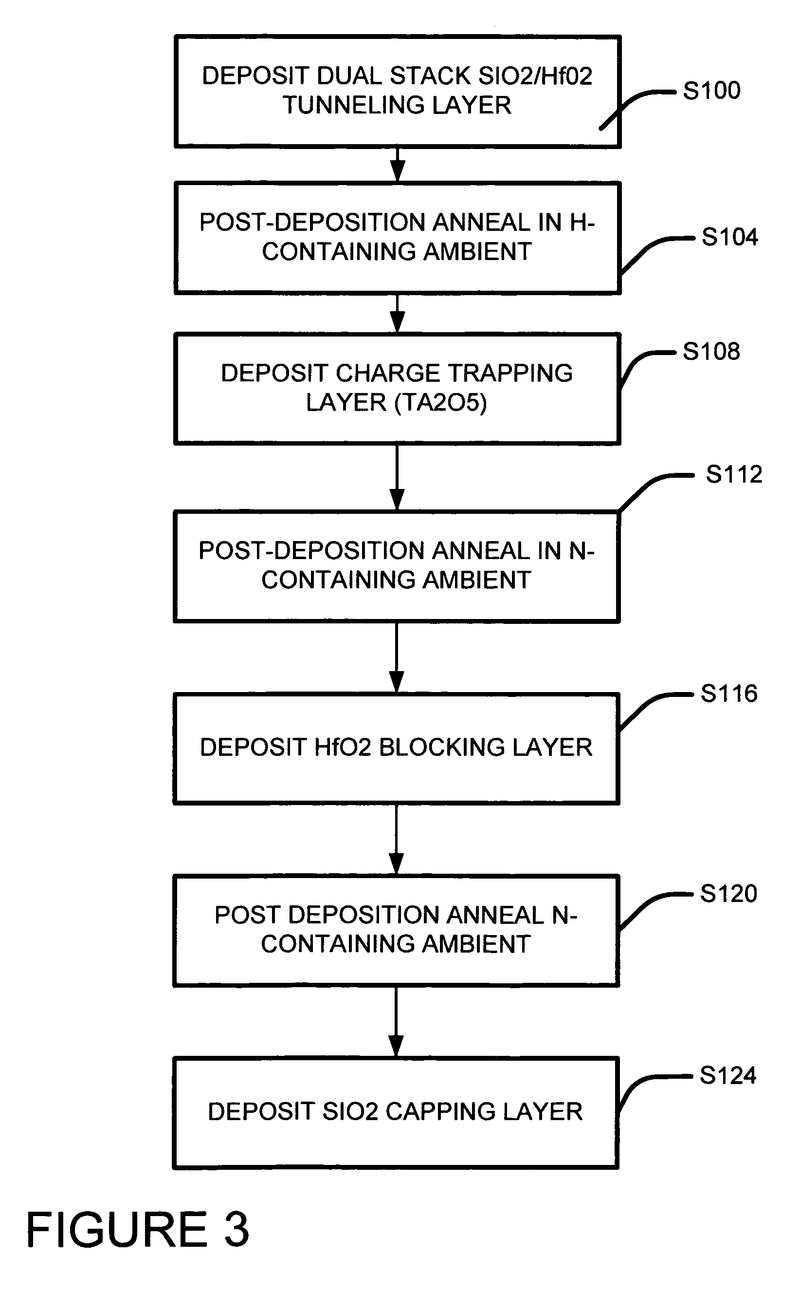
[0087] A second example embodiment is shown in FIG. 2 and the flowchart in FIG. 4. Corresponding layers and process can be carried out as described above in the first example embodiment.
[0088] The second example embodiment of a memory structure is depicted in FIG. 2. It preferably employs a top blocking layer 240 comprised of SiO2, a charge storage layer 232 comprised of Ta2O5, and a bottom tunnel dielectric 228 comprised of SiO2. The gate electrode 244 can be metal or polysilicon.
A. A Bottom Tunnel Layer
[0089] We provide a substrate. We form a bottom tunnel layer 228 over a substrate 210.
[0090] The bottom tunnel layer 228 is preferably comprised essentially of silicon oxide and has a thickness between 1 and 4 nm and more preferably about 2 nm.
B. Bottom Layer Anneal Step
[0091] Referring to FIG. 4, step 204, in an optional tunnel nitridation step, annealing the bottom tunnel layer 28 in a nitrogen and hydrogen containing atmosphere.
[0092] The tunn...
PUM
 Abstract
Description
Claims
Application Information
 - R&D
- Intellectual Property
- Life Sciences
- Materials
- Tech Scout
- Unparalleled Data Quality
- Higher Quality Content
- 60% Fewer Hallucinations
Browse by: Latest US Patents, China's latest patents, Technical Efficacy Thesaurus, Application Domain, Technology Topic, Popular Technical Reports.
© 2025 PatSnap. All rights reserved.Legal|Privacy policy|Modern Slavery Act Transparency Statement|Sitemap|About US| Contact US: help@patsnap.com


