Photo-detection device and manufacturing method thereof

Inactive Publication Date: 2006-07-13
HAMAMATSU PHOTONICS KK
View PDF10 Cites 10 Cited by
  • Summary
  • Abstract
  • Description
  • Claims
  • Application Information

AI Technical Summary

Benefits of technology

[0009] Since the semiconductor substrate and the cooling device are housed within a single package as mentioned above, this photodetection device can be made compact. Also, since the cooling surface of the cooling device contacts the front surface of the semiconductor substrate, on which the CCD reading part is provided, so as to cover the region at which the CCD reading part is formed, the CCD reading part can be cooled directly using the cooling device.
[0022] After the wire bonding work, the working openings are preferably closed with covers. Likewise, preferably after the wire bonding work, the upper opening of the cavity is closed by a top plate. By thus closing the upper opening of the cavity by a top plate, the interior of the cavity can be readily filled with an inert gas atmosphere or kept in a vacuum state, both of which are effective in terms of preventing dew condensation in the cavity.

Problems solved by technology

The conventional back-illuminated type photodetection device was thus poor in cooling efficiency and had an issue in that a cooling member 107 of high cooling capacity (and thus of large size) had to be used.

Method used


Image

  • Photo-detection device and manufacturing method thereof
  • Photo-detection device and manufacturing method thereof
  • Photo-detection device and manufacturing method thereof

Examples


Embodiment Construction

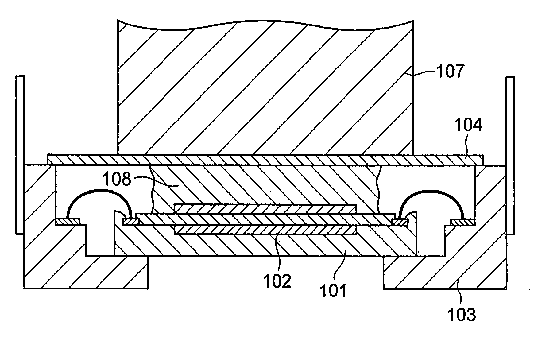
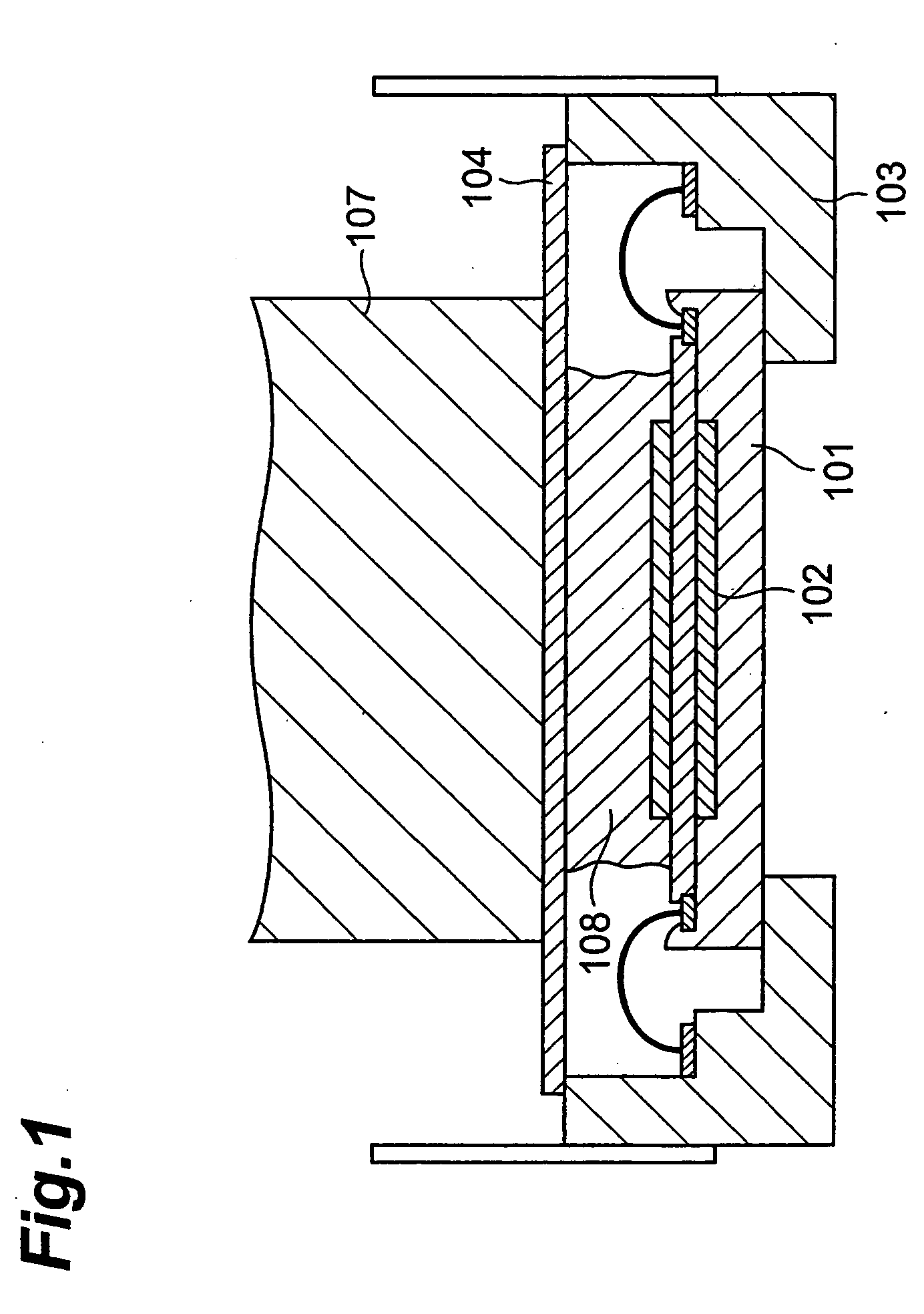
[0031] Embodiments of a photodetection device and a manufacturing method therefore according to the present invention shall now be described in detail using FIGS. 2 to 4 and 5A to 6C. In the description of the drawings, the same symbols shall be attached to portions and elements that are the same and redundant description shall be omitted.

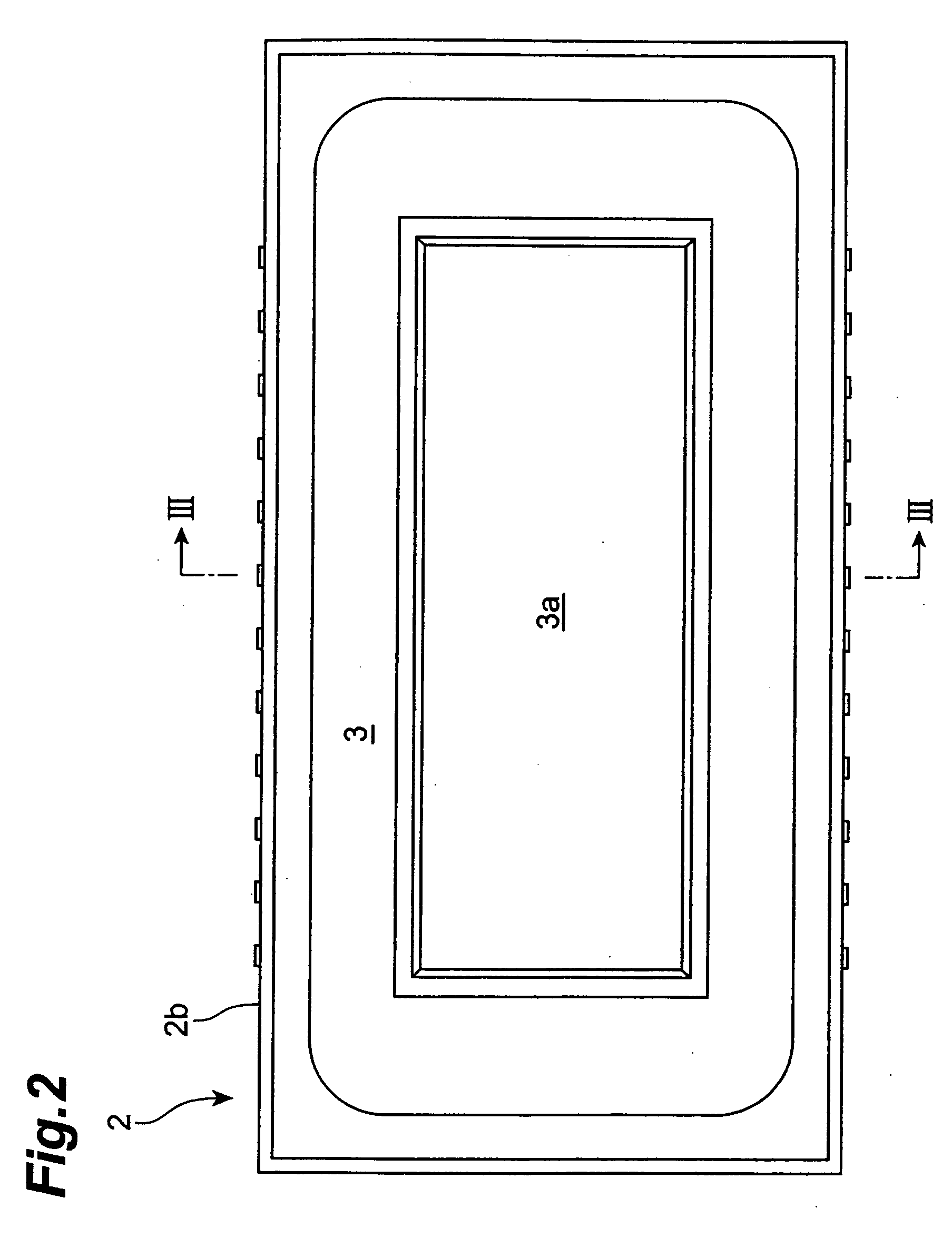
[0032]FIG. 2 is a plan view of a photodetection device according to the present invention as viewed from an upper part side (back surface side of a semiconductor substrate onto which light is made incident), FIG. 3 is a plan view of the photodetection device of FIG. 2 as viewed from a bottom part side (front surface side of the semiconductor substrate), and FIG. 4 is a diagram showing the cross sectional structure of the photodetection device according to the present invention taken along line III-III in FIG. 2.

[0033] The photodetection device according to the present invention is equipped with a package 2, having a cavity 2f surrounded by a bott...


PUM


Abstract

This invention relates to a photodetection device, etc., equipped with a structure that efficiently cools a CCD reading part and can realize a downsizing of the entire device. The photodetection device comprises: a semiconductor substrate having a back surface which serves as a light-incident surface, and a front surface which opposes the back surface and is provided with a CCD reading part that detects light propagating from the back surface; a cooling device cooling the CCD reading part; and a package having a cavity that houses the semiconductor substrate and cooling device. The semiconductor substrate is fixed to a cavity bottom part of the package via the cooling device, and at the back surface thereof, a portion corresponding to a region at which the CCD reading part is disposed, is made thin. The cooling device has a cooling surface contacting the front surface of the semiconductor substrate while covering the region at which the CCD reading part is disposed. The size of the cooling surface is larger than the region at which the CCD reading part is disposed and yet smaller than the front surface of the semiconductor substrate. Also, electrode pads, disposed on the front surface of the semiconductor substrate and positioned at the peripheral of the region covered by the cooling surface of the cooling device, and package terminals provided on the package are electrically connected via bonding wires.

Description

TECHNICAL FIELD [0001] This invention relates to a photodetection device, in particular, a back-illuminated type photodetection device, with which light that has been made incident from a back surface is detected using a photoelectric conversion element disposed on a front surface that opposes the back surface, and a method of manufacturing such a photodetection device. BACKGROUND ART [0002] A photodetection device (referred to hereinafter as “back-illuminated type photodetection device”), with which light that has been made incident on a back surface and has been transmitted through a semiconductor substrate is detected by a charge reading part (referred to hereinafter as “CCD reading part”), comprising a charge-coupled device disposed on a front surface of the semiconductor substrate, has good sensitivity down to shorter wavelengths in comparison to a photodetection device (referred to hereinafter as “front-illuminated type photodetection device”), with which incident light is det...

Claims


Application Information

Patent Timeline
IPC IPC(8): H01L21/00H01L33/00G01J1/02F25B21/02F25D19/00H01L27/14H01L27/146H01L27/148H01L31/024
CPCF25B21/02F25D19/006H01L27/14618H01L27/14683H01L27/14806H01L27/1464H01L2224/48091H01L2224/49175H01L31/024H01L2924/00014H01L2224/05553H01L2924/10158
Inventor KOBAYASHI, HIROYAMURAMATSU, MASAHARU
Owner HAMAMATSU PHOTONICS KK
Why Eureka
Try Eureka