
Producing method for electron-emitting device and electron source, and image display apparatus utilizing producing method for electron-emitting device

a technology of electron emission device and producing method, which is applied in the manufacture of electrode systems, electric discharge tubes/lamps, and discharge tubes luminescent screens, etc., can solve the problems of reducing the contrast of displayed images, difficult control of electrons, and difficult to produce, and achieves convenient and fast production. , the effect of reducing the cost of production

Inactive Publication Date: 2006-06-15
CANON KK
View PDF9 Cites 22 Cited by
  • Summary
  • Abstract
  • Description
  • Claims
  • Application Information

AI Technical Summary

Benefits of technology

The patent text describes a problem with electron-emitting devices that use semiconductors with negative electron affinity or very small positive electron affinity. These devices tend to have a "half-selection current" where some electrons are emitted but not all of them are emitted. This results in unintended light emission and reduces the contrast of the displayed image. The patent proposes a solution to this problem by controlling the electron injection and emission through a matrix of X and Y direction wirings. The "technical effect" of this solution is to improve the control of electron emission and reduce the unintended light emission, resulting in a higher contrast ratio in the display.

Problems solved by technology

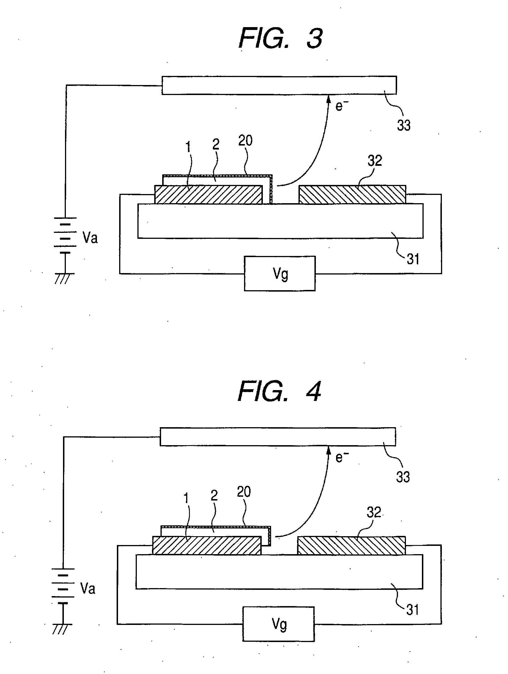
Because of such property of very easily emitting the electrons, it may become very difficult, in an application to a display or an electron source, to control the electron emission amount (particularly on-off switching) from each electron-emitting device.
Consequently, in an application to the image display apparatus such as television, an unintended pixel (light-emitting member) causes a light emission with an unintended light intensity thereby reducing a contrast of a displayed image.

Method used


Image

  • Producing method for electron-emitting device and electron source, and image display apparatus utilizing producing method for electron-emitting device
  • Producing method for electron-emitting device and electron source, and image display apparatus utilizing producing method for electron-emitting device
  • Producing method for electron-emitting device and electron source, and image display apparatus utilizing producing method for electron-emitting device

Examples


example 1

[0146] An electron emitting film was prepared according to the producing method shown in FIGS. 17A to 17D.

[0147] Quartz was employed as the substrate 31, which was rinsed well and subjected to formation of a TiN film of a thickness of 500 nm as the cathode electrode 1 by sputtering (FIG. 17A). The employed film forming conditions were as follows: [0148] Rf power source: 13.56 MHz [0149] Rf power: 7.7 W / cm2 [0150] gas pressure: 0.6 Pa [0151] gas atmosphere: N2 / Ar (N2:10%) [0152] substrate temperature: room temperature [0153] target: Ti

[0154] Then, on the cathode electrode 1, Pt eloctroconductive particles 7 were formed, as shown in FIG. 17B, by sputtering under following conditions: [0155] Rf power source: 13.56 MHz [0156] Rf power: 300 W [0157] gas atmosphere: Ar [0158] substrate temperature: 150° C. [0159] target: Pt

[0160] An observation of the surface of the cathode electrode 1 under an electron microscope revealed that fine Pt particles of an average particle size of 10 nm wer...

example 2

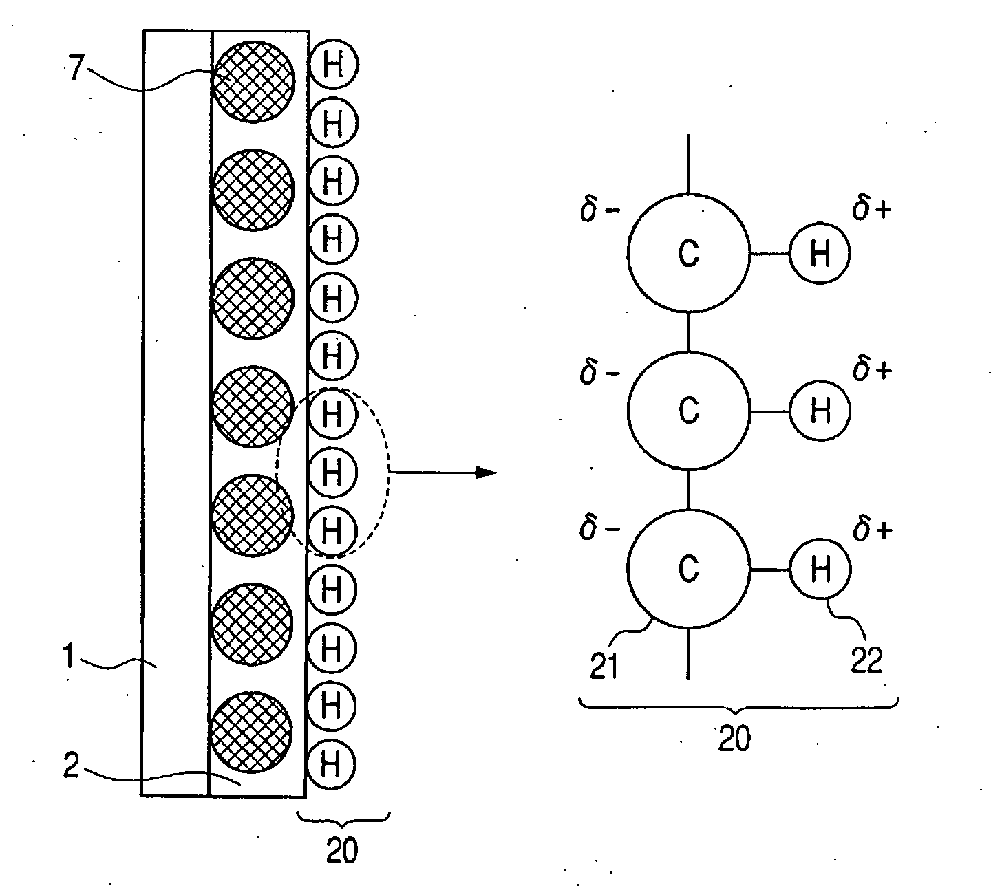
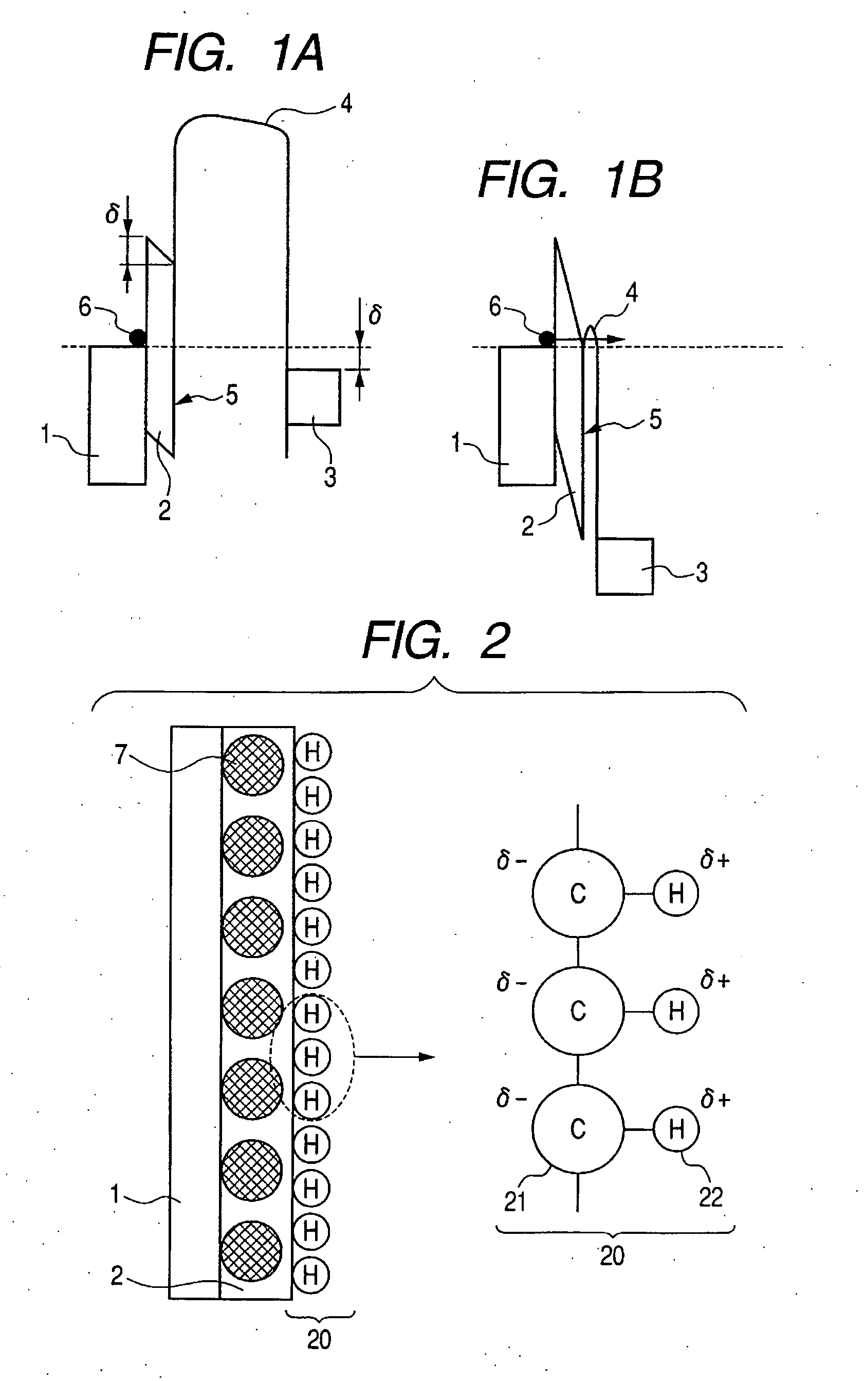
[0176] An insulation layer 2 of the present invention including electroconductive particles 7 and provided with a dipole layer 20 was prepared according to the producing method shown in FIGS. 17A to 17D.

[0177] Quartz was employed as the substrate 31, which was rinsed well and subjected to formation of a W film of a thickness of 500 nm as the cathode electrode 1 by sputtering (FIG. 17A).

[0178] Then, on the cathode electrode 1, Co electroconductive particles 7 were formed, as shown in FIG. 17B, by sputtering under following conditions: [0179] Rf power source: 13.56 MHz [0180] Rf power: 300 W [0181] gas atmosphere: Ar [0182] substrate temperature: 150° C. [0183] target: Co

[0184] An observation of the surface of the cathode electrode 1 under an electron microscope revealed that fine Co particles of an average particle size of 6 nm were formed with a density of 1×10⁶ / mm2 on the cathode electrode 1.

[0185] Then SiO2 was deposited on the cathode electrode 1 by 5 nm by sputtering to form...

example 3

[0197] As in Example 1, quartz was employed as the substrate 31, which was rinsed well and subjected to formation of a TiN film of a thickness of 500 nm as the cathode electrode 1 by sputtering.

[0198] Then on the cathode electrode 1, a Pt film of a thickness of 15 nm was formed by sputtering under following conditions: [0199] Rf power source: 13.56 MHz [0200] Rf power: 300 W [0201] gas atmosphere: Ar [0202] substrate temperature: room temperature [0203] target: Pt

[0204] Then the Pt film was heated in a hydrogen atmosphere to form granules. An observation of the surface of the cathode electrode 1 revealed that Pt particles of an average particle size of 20 nm were formed with a density of 4×10⁷ / mm2 on the cathode electrode 1.

[0205] Then a carbon film was formed by inclined evaporation on the cathode electrode 1 and the Pt particles 7, thereby forming an insulation layer 2 of a carbon film. The carbon film was formed on the electroconductive particles 7 and the cathode electrode 1,...


PUM


Abstract

The invention is to provide a producing method for an electron emitting device of field emission type, having sufficient on / off characteristics and capable of efficient electron emission at a low voltage. There is provided a producing method for an electron emitting device including steps of preparing a plurality of electroconductive particles each covered with an insulation material having a thickness of 10 nm or less at least on a part of a surface of the particle, and forming a dipole layer on a surface of the insulation material covering each of the plurality of electroconductive particles.

Description

[0001] This application claims priority from Japanese Patent Application No. 2004-358362 filed on Dec. 10, 2004, which is hereby incorporated by reference herein. BACKGROUND OF THE INVENTION [0002] 1. Field of the Invention [0003] The present invention relates to a producing method for an electron emitting device of field emission type, a producing method for an electron source formed by arranging a plurality of the electron emitting devices, and a producing method for an image display apparatus, such as a television, formed by employing the electron source. [0004] 2. Related Background Art [0005] An electron-emitting device includes, for example, a field emission type (hereinafter called FE type) and a surface conduction type. [0006] The electron-emitting device of FE type is of a type in which a voltage is applied between a cathode electrode (and an electron-emitting film provided thereon) and a gate electrode thereby extracting, by such voltage (electric field), electrons from th...

Claims


Application Information

Patent Timeline
Patent Type & Authority Applications(United States)
IPC IPC(8): H01J1/304
CPCH01J1/316H01J9/027H01J31/127H01J2201/3165
Inventor NISHIMURA, MICHIYOTERAMOTO, YOJIFUJIWARA, RYOJI
Owner CANON KK
Learn More