Semiconductor light emitting diode having high efficiency and method of manufacturing the same
- Summary
- Abstract
- Description
- Claims
- Application Information
AI Technical Summary
Benefits of technology
Problems solved by technology
Method used
Image

Examples
Embodiment Construction
[0028] The present invention will now be described more fully with reference to the accompanying drawings, in which exemplary embodiments of the invention are shown.
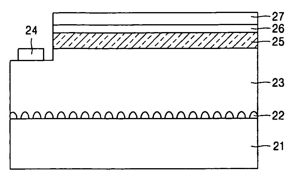
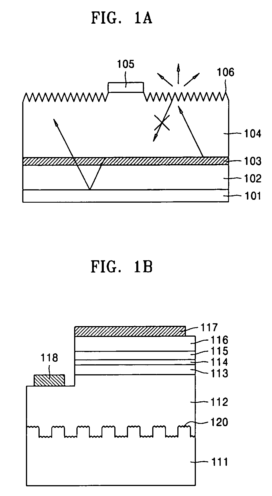
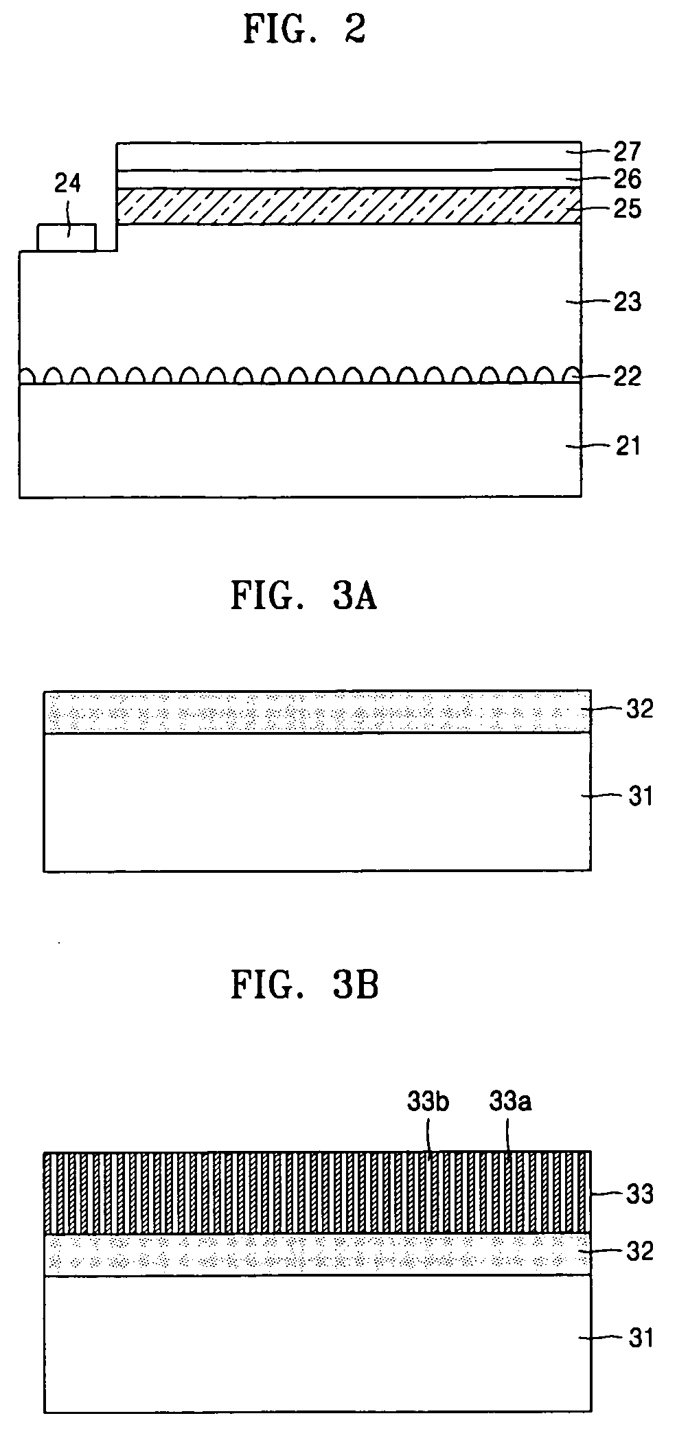
[0029]FIG. 2 is a cross-sectional view illustrating the structure of a semiconductor light emitting diode having a textured structure according to an embodiment of the present invention. Referring to FIG. 2, a textured structure layer 22 and a first semiconductor layer 23 are formed on a substrate 21. An active layer 25 and a second semiconductor layer 26 are formed on the first semiconductor layer 23, and a first electrode 24 is formed on the first semiconductor layer 23 where the active layer 25 is not formed. A second electrode 27 is formed on the second semiconductor layer 26.
[0030] The textured structure layer 22 is formed with a non-planar structure between the substrate 21 and the first semiconductor layer 23. The textured structure layer 22 is incorporated to increase light extraction efficiency by changing the...
PUM
 Abstract
Description
Claims
Application Information
 - R&D
- Intellectual Property
- Life Sciences
- Materials
- Tech Scout
- Unparalleled Data Quality
- Higher Quality Content
- 60% Fewer Hallucinations
Browse by: Latest US Patents, China's latest patents, Technical Efficacy Thesaurus, Application Domain, Technology Topic, Popular Technical Reports.
© 2025 PatSnap. All rights reserved.Legal|Privacy policy|Modern Slavery Act Transparency Statement|Sitemap|About US| Contact US: help@patsnap.com