
Organic light emitting display and method for fabricating the same

a technology of light-emitting diodes and display panels, which is applied in the direction of discharge tubes/lamp details, discharge tubes luminescnet screens, electric discharge lamps, etc., can solve the problems of degrading efficiency of top-emitting oled displays, and achieve the effect of long life and high efficiency

Active Publication Date: 2006-06-01
SAMSUNG DISPLAY CO LTD
View PDF19 Cites 93 Cited by
  • Summary
  • Abstract
  • Description
  • Claims
  • Application Information

AI Technical Summary

Benefits of technology

[0014] The embodiments of the present invention provide an OLED display with high efficiency and long lifetime by depositing an organic capping layer having a refractive index of at least 1.7 on a second electrode.

Problems solved by technology

However, as the passivation layer is deposited without any consideration of its refractive index and thickness, the top-emitting OLED display degrades in efficiency.

Method used


Image

  • Organic light emitting display and method for fabricating the same
  • Organic light emitting display and method for fabricating the same
  • Organic light emitting display and method for fabricating the same

Examples


embodiment 1

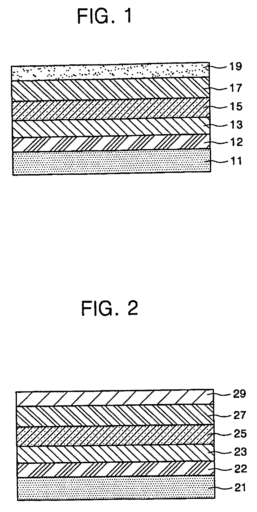
[0053] A glass substrate was prepared. A reflecting layer of a first electrode was formed of Al on the substrate, and ITO was deposited on the reflecting layer of Al. An organic layer was then formed on the ITO by depositing m-TDATA in a hole injection layer, NPB in a hole transport layer, red-CBP:BTPIr, green-CBP:Ir ppy 3 and blue-Alq3:DPBVi in an emission layer, BaIq in a hole blocking layer, Alq3 in an electron transport layer, and LiF in an electron injection layer. MgAg was deposited as a second electrode, and then an organic capping layer having a thickness of 200 Å was deposited by performing vacuum deposition on an arylenediamine derivative having a 1.7 or more refractive index in conditions of 280 to 300° C. in temperature, about 10e−7 in vacuum and 1 Å / sec in a deposition rate, thus completing the top-emitting OLED display.

embodiment 2

[0054] A top-emitting OLED display was formed as in Embodiment 1 except that an organic capping layer was deposited to a thickness of 400 Å.

embodiment 3

[0055] A top-emitting OLED display was formed as in Embodiment 1 except that an organic capping layer was deposited to a thickness of 600 Å.


PUM


Abstract

An organic light emitting diode (OLED) display and a method for fabricating the same. The OLED display includes: a substrate; a first electrode formed on the substrate and including a reflecting layer; an organic layer formed on the first electrode and including at least an organic emission layer; a second electrode formed on the organic layer; and an organic capping layer formed on the second electrode. The organic capping layer is formed by stacking an organic material having a refractive index of 1.7 or more, thereby providing a high-efficiency and long-life top-emitting OLED display.

Description

CROSS-REFERENCE TO RELATED APPLICATION [0001] This application claims priority to and the benefit of Korean Patent Application No. 10-2004-0098238, filed Nov. 26, 2005, the entire content of which is incorporated herein by reference. BACKGROUND OF THE INVENTION [0002] 1. Field of the Invention [0003] The present invention relates to an organic light emitting diode (OLED) display and a method for fabricating the same, and more particularly, to an OLED display and a method for fabricating the same in which an organic capping layer having a refractive index of 1.7 or more is formed on a second electrode of the OLED display. [0004] 2. Description of the Related Art [0005] Among flat panel displays, an organic light emitting diode (OLED) display is an emission display that emits light by electrically exciting an organic compound. As used herein OLED display may refer to a single OLED, multiple OLEDs or an OLED display device. The OLED display requires no backlight, which is used in a liq...

Claims


Application Information

Patent Timeline
Patent Type & Authority Applications(United States)
IPC IPC(8): H01L51/00H10K99/00
CPCH01L51/5237H10K59/879H10K59/873H05B33/22H05B33/10H10K50/858H10K50/844
Inventor IM, JA-HYUNLEE, KWAN-HEERYU, SEOUNG-YOON
Owner SAMSUNG DISPLAY CO LTD
Learn More