Semiconductor device and method for controlling the same

a technology of semiconductor devices and semiconductors, applied in the field of semiconductor devices, can solve the problems of poor usability, slow data rewriting, and inability to rewrite data, and achieve the effect of high-speed operation and sufficient operating margin

Active Publication Date: 2006-05-25
MONTEREY RES LLC
View PDF11 Cites 0 Cited by
  • Summary
  • Abstract
  • Description
  • Claims
  • Application Information

AI Technical Summary

Benefits of technology

[0014] The present invention has an object of overcoming the above-mentioned problems of the conventional flash memory equipped with the dual-operation function and providing a technique capable of assuring high-speed operation and sufficient operating margin regardless of the dual operation mode.

Problems solved by technology

With the miniaturization of the device, the cell current Ic inevitably decreases.
In the conventional flash memory, data rewriting is slow and the usability is poor as compared to the DRAM or SRAM because of the following.
In the flash memory, read operation by the processor is not allowed when programming or erasing is in progress.

Method used


Image

  • Semiconductor device and method for controlling the same
  • Semiconductor device and method for controlling the same
  • Semiconductor device and method for controlling the same

Examples


Embodiment Construction

[0032] A semiconductor memory device according to an aspect of the present invention will now be described with reference to the accompanying drawings. In the semiconductor memory device in the following description is a NOR type flash memory.

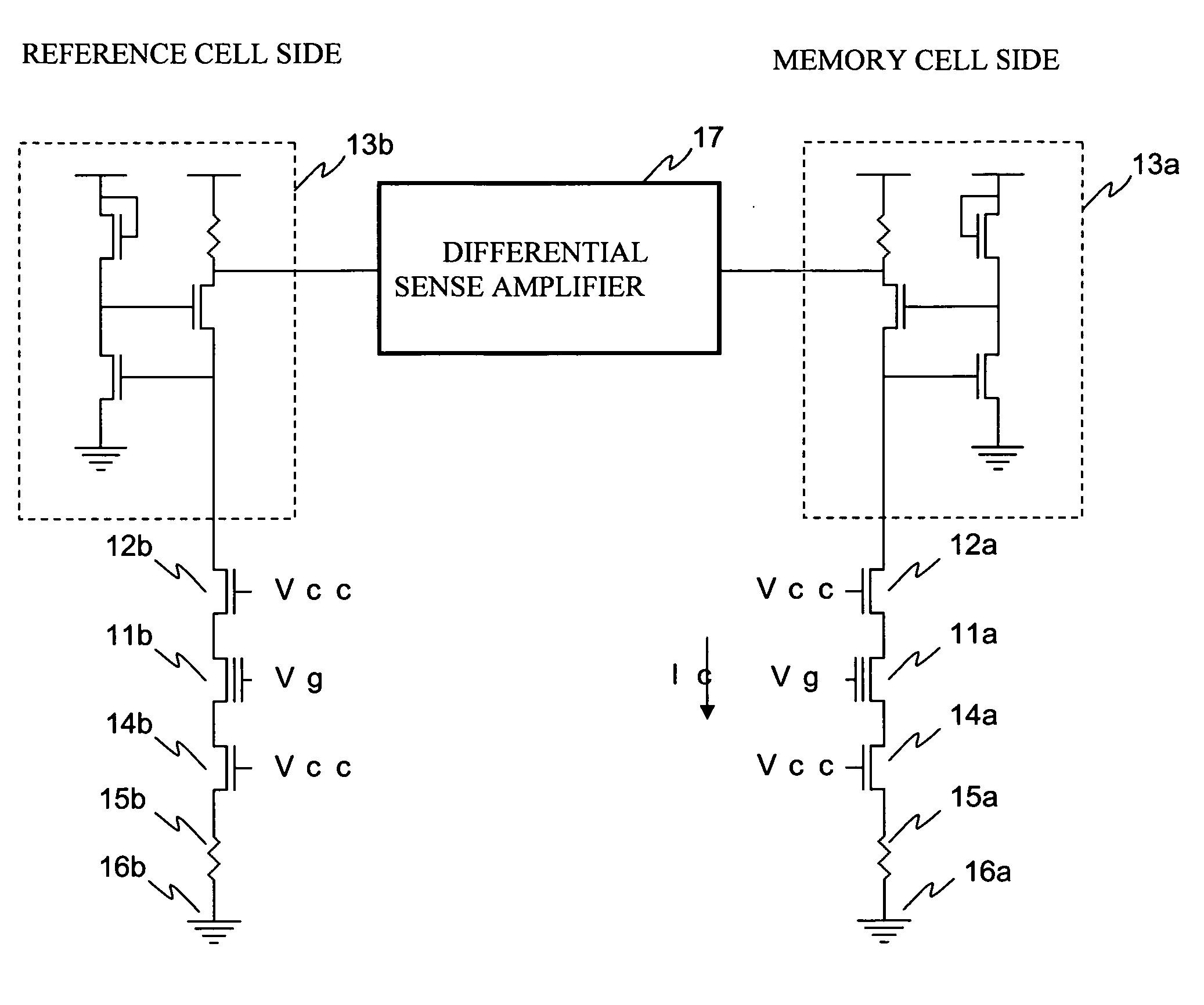
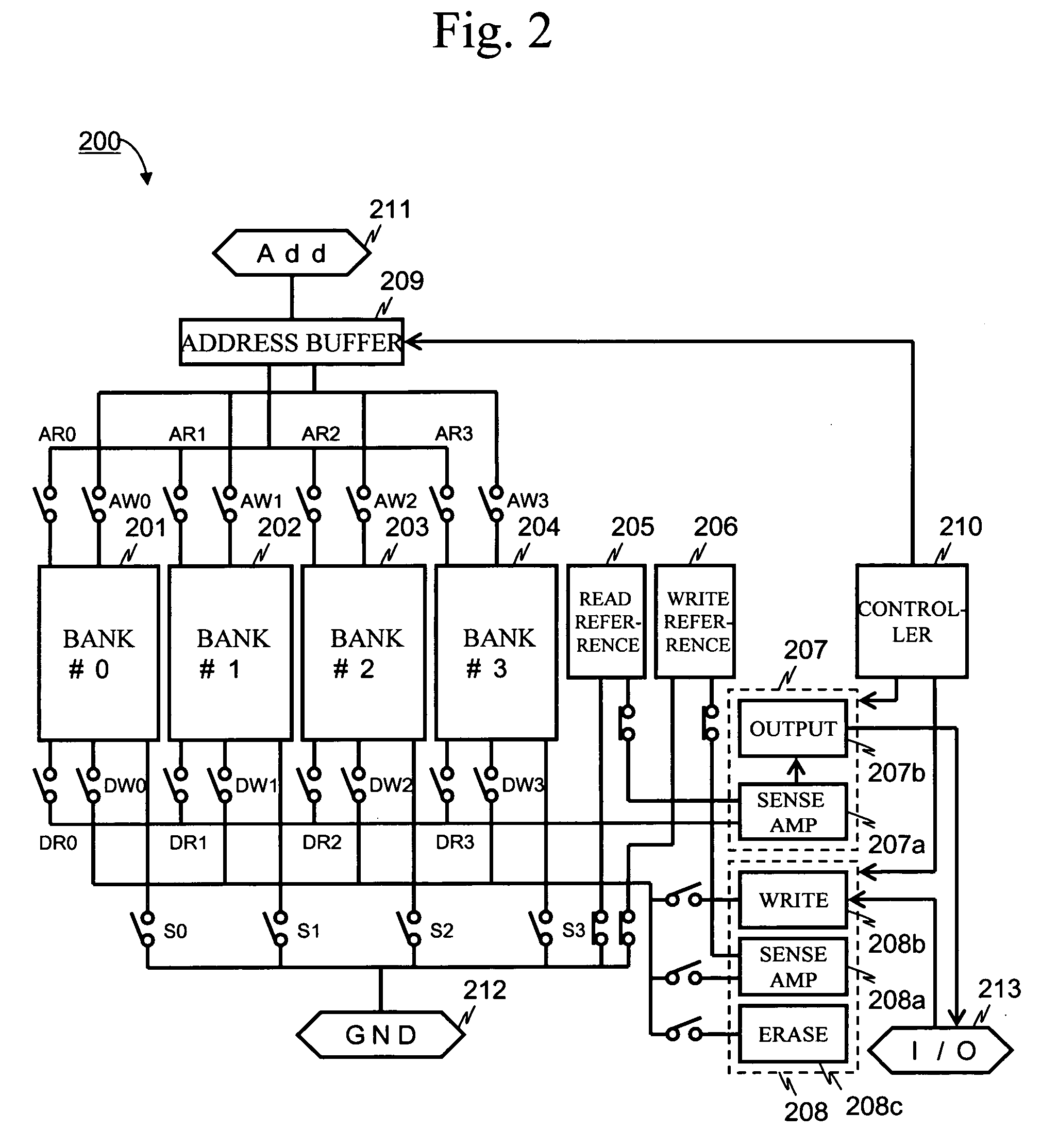
[0033]FIG. 3 is a block diagram of an internal configuration of the flash memory according to an aspect of the present invention. The flash memory is separately equipped with a read ground 312a and a write ground 312b for verification. This makes the source potential of the memory cell equal to that obtained when only one of the read and verify operations is executed even when the read and verify operations are concurrently executed. It is thus possible to realize high-speed read operation stabilized due to an enhanced read margin irrespective of whether the device is in the dual operation mode.

[0034] A memory cell array 300 has four banks of a zeroth bank 301, a first bank 302, a second bank 303 and a third bank 304. The memory cell array 20...


PUM


Abstract

A semiconductor memory device has a read ground and a write ground, these grounds being separately provided. Even when the read and verify operations are simultaneously executed, the source potential of an involved memory cell obtained at this time is equal to that obtained when either one of the read and verify operations is executed. Thus, the semiconductor memory device can perform the read operation at high speed with a sufficient operating margin regardless of whether the device is in the dual operation mode or not.

Description

CROSS REFERENCE TO RELATED APPLICATIONS [0001] This is a continuation of International Application No. PCT / JP2004 / 014326, filed Sep. 30, 2004. BACKGROUND OF THE INVENTION [0002] 1. Field of the Invention [0003] The present invention relates to a semiconductor device, and more particularly, a technique for achieving high-speed operation and a sufficient operating margin of a semiconductor memory having a dual operation function. [0004] 2. Description of the Related Art [0005] Recently, the flash memory has come into wide use as an electrically rewritable semiconductor memory device. The flash memory is categorized into the NAND type used for data storage that is typically the memory card, and the NOR type that stores a program and is built in electronic devices. The typical NOR type flash memory stores data (“1” or “0”) based on whether the charge is stored in the floating gate. The unit cell of the NOR type flash memory is composed of a single MOS transistor, which is equipped with ...

Claims


Application Information

Patent Timeline
Patent Type & Authority Applications(United States)
IPC IPC(8): G11C16/04
CPCG11C16/06G11C16/28G11C16/3436G11C16/3459G11C2216/22
Inventor KITAZAKI, KAZUHIRO
Owner MONTEREY RES LLC
Why Eureka
Try Eureka