
Apparatus for removing DC offset and amplifying signal with variable gain simutaneously

Inactive Publication Date: 2006-05-25
SUNPLUS TECH CO LTD
View PDF6 Cites 0 Cited by
  • Summary
  • Abstract
  • Description
  • Claims
  • Application Information

AI Technical Summary

Benefits of technology

[0012] The present invention is directed to an apparatus for removing DC offset and amplifying signal with variable gain simultaneously without occupying a large surface area of an IC substrate and thereby simplifying the circuit design.
[0023] The present invention employs the low-pass filter to segregate DC offset from the normal input signal, wherein a frequency of the DC offset is lower than that of the normal input signal, and thereby achieve the purpose of removing the DC offset and amplifying signal with variable gain simultaneously. Furthermore, all capacitors used in the present invention can employ a metal-oxide-semiconductor field effect transistor (MOS FET), and therefore the consumption of the surface area of the substrate can be effectively reduced.

Problems solved by technology

An amplifier with a variable gain would saturate when a phenomenon of DC offset occurs, which inhibits the amplifier from achieving its amplifying effect and thus raises a bit-error-rate of the receiver, even resulting in failure of receiving a signal by the receiver.
However, since the two terminals of the capacitor are not connected to ground, it is required to employ a metal-insulator-metal (MIM) capacitor or a polysilicon-insulator-polysilicon (PIP) capacitor with a large capacitance, however these two capacitors occupy a large surface area of an IC substrate and thus cause a problem of an IC design.
However, since none of the terminal of the capacitor is connected to ground, it is required to employ a MIM capacitor or a PIP capacitor with a large capacitance, however, these two capacitors also occupy a large surface area of an IC substrate and thus cause a problem in the IC design.
In conclusion, although by utilizing the ADC, DSP, and DAC or MIM and PIP capacitors, the DC offset can be removed, the complex circuit design and consumption of large surface area of the substrate by the capacitors make it inconvenient to practically apply in the circuit design.

Method used


Image

  • Apparatus for removing DC offset and amplifying signal with variable gain simutaneously
  • Apparatus for removing DC offset and amplifying signal with variable gain simutaneously
  • Apparatus for removing DC offset and amplifying signal with variable gain simutaneously

Examples


Embodiment Construction

[0030] Reference will now be made in detail to the present preferred embodiments of the invention, examples of which are illustrated in the accompanying drawings. Wherever possible, the same reference numbers are used in the drawings and the description to refer to the same or like parts.

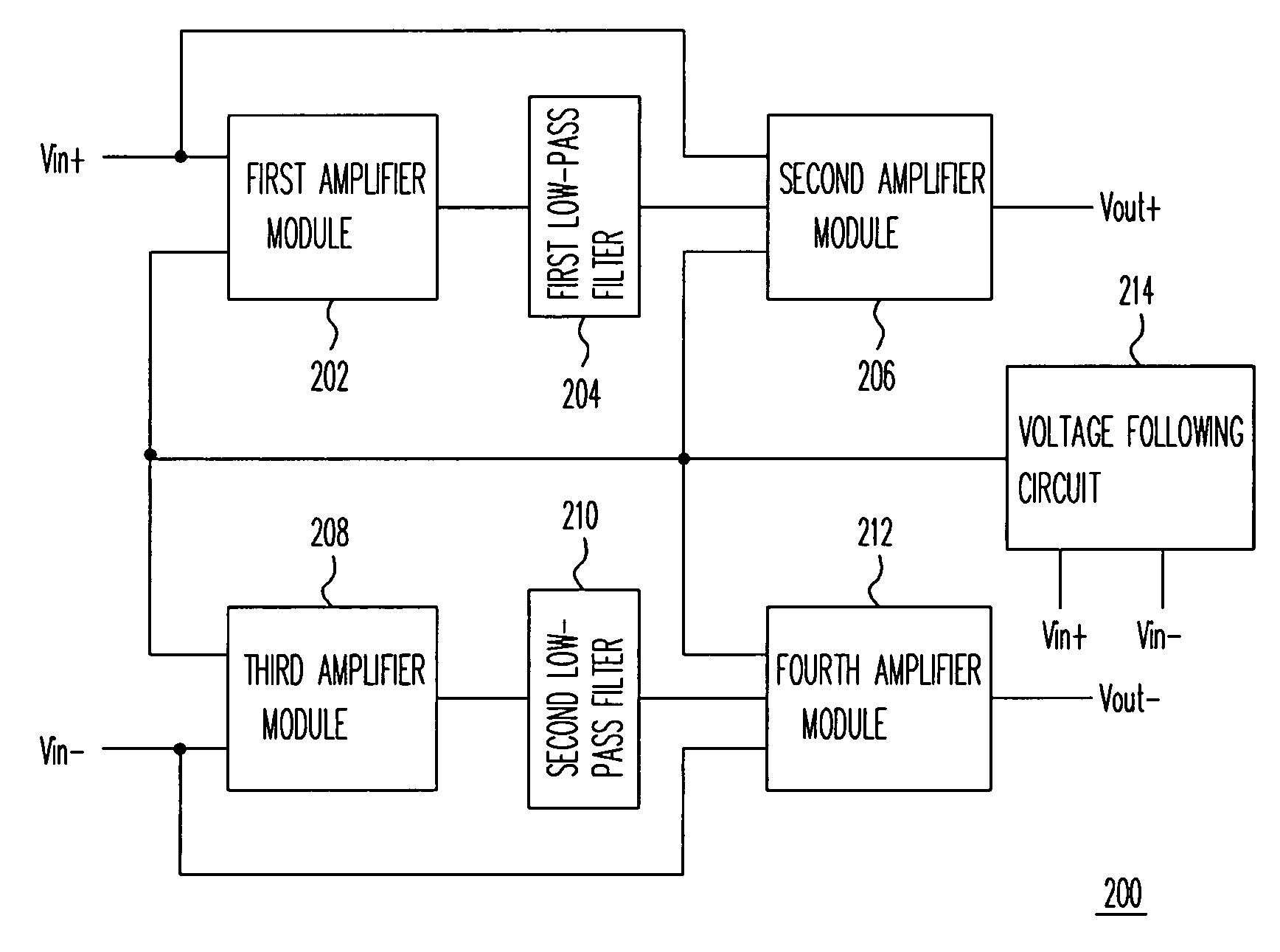
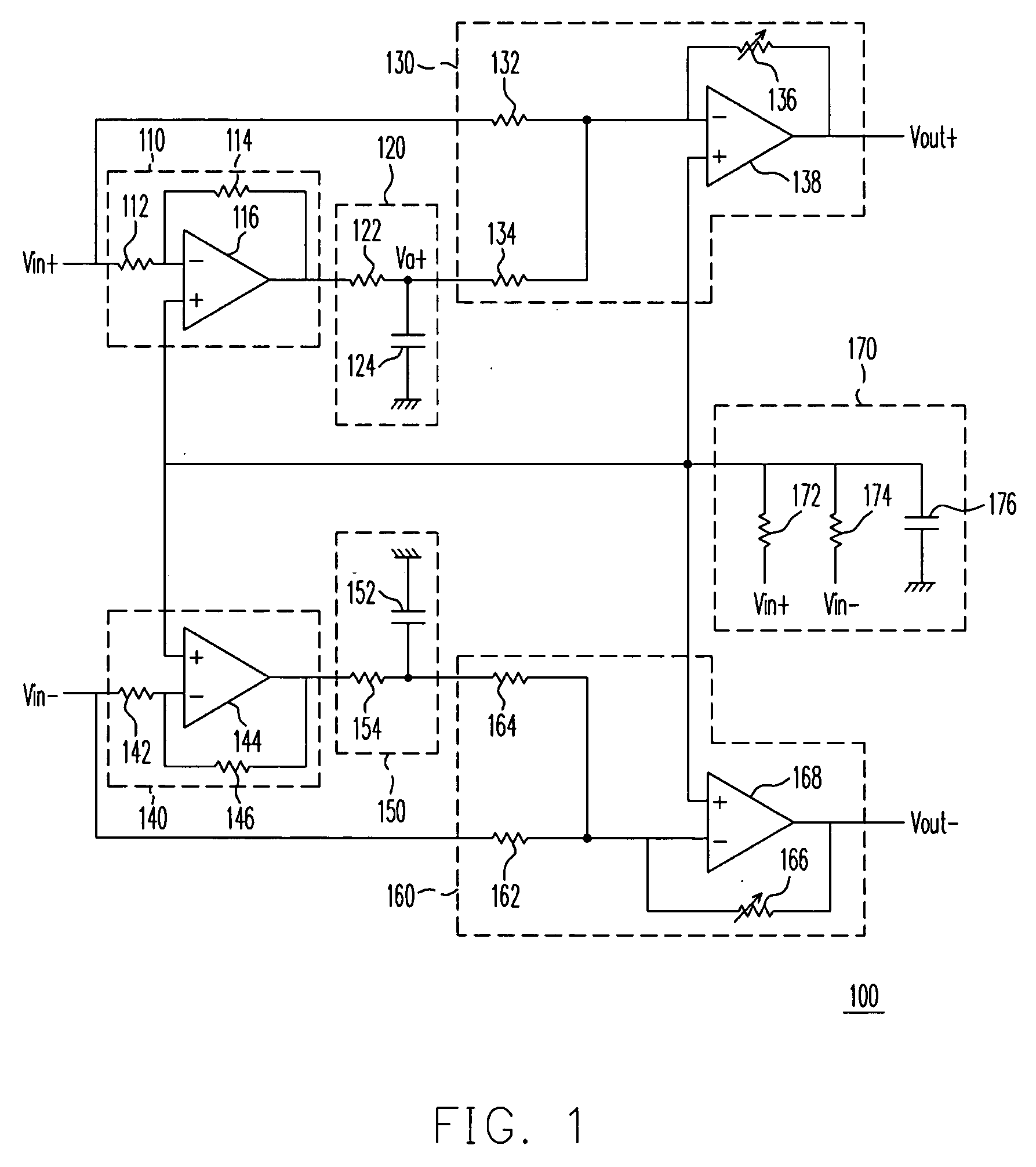
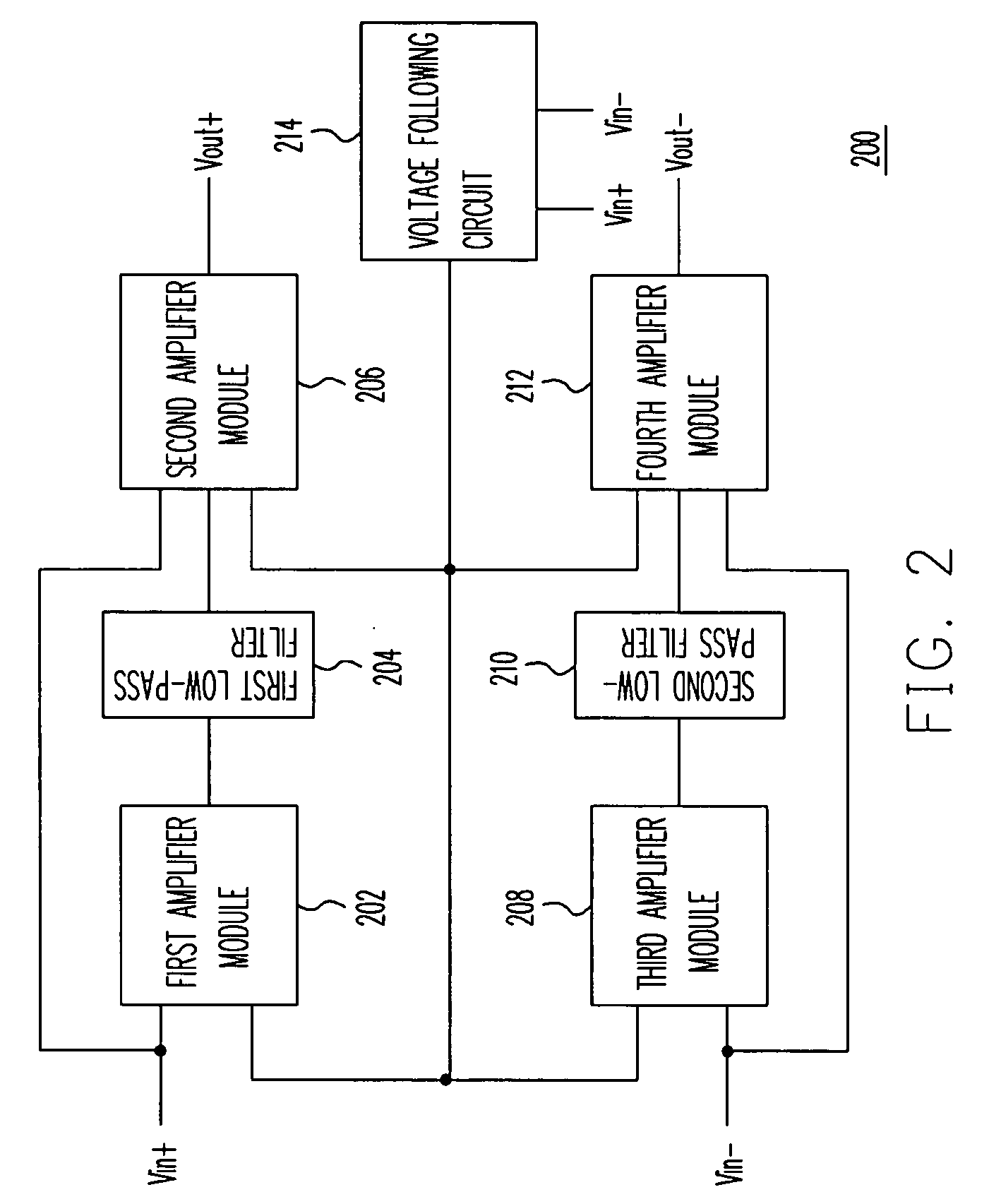
[0031] Referring to FIG. 1, a circuit diagram for removing DC offset and amplifying signal with variable gain simultaneously suitable for a zero frequency receiver in a communication receiving device according to an embodiment of the present invention is shown. Wherein a circuit 100 for removing DC offset and amplifying signal with variable gain simultaneously comprises a first amplifier module 110, a first filter circuit 120, a second amplifier module 130, a third amplifier module 140, a second filter circuit 150, a fourth amplifier module 160 and a voltage following circuit 170.

[0032] The first amplifier module 110 comprises a first resistance 112, a second resistance 114, and a first operationa...


PUM


Abstract

An apparatus for removing DC offset and variable gain amplifying simultaneously is provided. A signal voltage level of the output terminal of the first amplifier module is A times that of the first input terminal of the first amplifier module. A voltage level of an output DC offset signal of the first low-pass filter circuit is B times that of the input signal of the first low-pass filter circuit. The output signal of the second amplifier module is a sum of a C1-time amplified first input signal of the second amplifier module and a C2-time amplified second input signal of the second amplifier module, which satisfy the following equation: A×B×C1=−C2.

Description

CROSS-REFERENCE TO RELATED APPLICATION [0001] This application claims the priority benefit of Taiwan application serial no. 93136263, filed on Nov. 25, 2004. All disclosure of the Taiwan application is incorporated herein by reference. BACKGROUND OF THE INVENTION [0002] 1. Field of the Invention [0003] The present invention generally relates to an apparatus for removing DC offset, and particularly, to an apparatus for removing DC offset in a zero intermediate frequency receiver or a low intermediate frequency receiver. [0004] 2. Description of Related Art [0005] A DC offset always occurs in a communication IC receiver configuration when operating at a zero intermediate frequency or a low intermediate frequency. Especially, it happens in a zero intermediate frequency receiver. [0006] An amplifier with a variable gain would saturate when a phenomenon of DC offset occurs, which inhibits the amplifier from achieving its amplifying effect and thus raises a bit-error-rate of the receiver,...

Claims


Application Information

Patent Timeline
IPC IPC(8): H03F3/45
CPCH03F1/34H03F3/45475H03F3/45968H03F2203/45522
Inventor CHUNG, YUAN-HUNG
Owner SUNPLUS TECH CO LTD
Learn More