Memory and semiconductor device

a technology applied in the field of memory and semiconductor devices, can solve the problems of difficult data overwriting at a high speed, long time necessary for erasing, and long time necessary for recording, so as to reduce the time necessary for writing and erasing

Inactive Publication Date: 2006-05-04
SONY CORP
View PDF4 Cites 13 Cited by
  • Summary
  • Abstract
  • Description
  • Claims
  • Application Information

AI Technical Summary

Benefits of technology

[0026] The present invention is made in consideration of the above disadvantages and it is desirable to provide a memory and a semiconductor device which are capable of reducing time necessary for writing and erasing.
[0032] According to the memory and the semiconductor device according to the embodiments of the present invention, whether a memory element is changed to a desired state can be detected during a write sequence or an erase sequence. Advantageously, a read sequence which has been necessary and follows the write sequence or the erase sequence is not needed. Thus, time necessary for writing and that for erasing can be reduced.

Problems solved by technology

Disadvantageously, this results in a long time necessary for recording.
For example, it is difficult to overwrite data at a high speed.
Similar to the write operation, therefore, two sequences have to be performed as the erasing operation including the verify step, resulting in a long time necessary for erasing.

Method used


Image

  • Memory and semiconductor device
  • Memory and semiconductor device
  • Memory and semiconductor device

Examples


Embodiment Construction

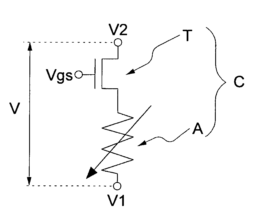
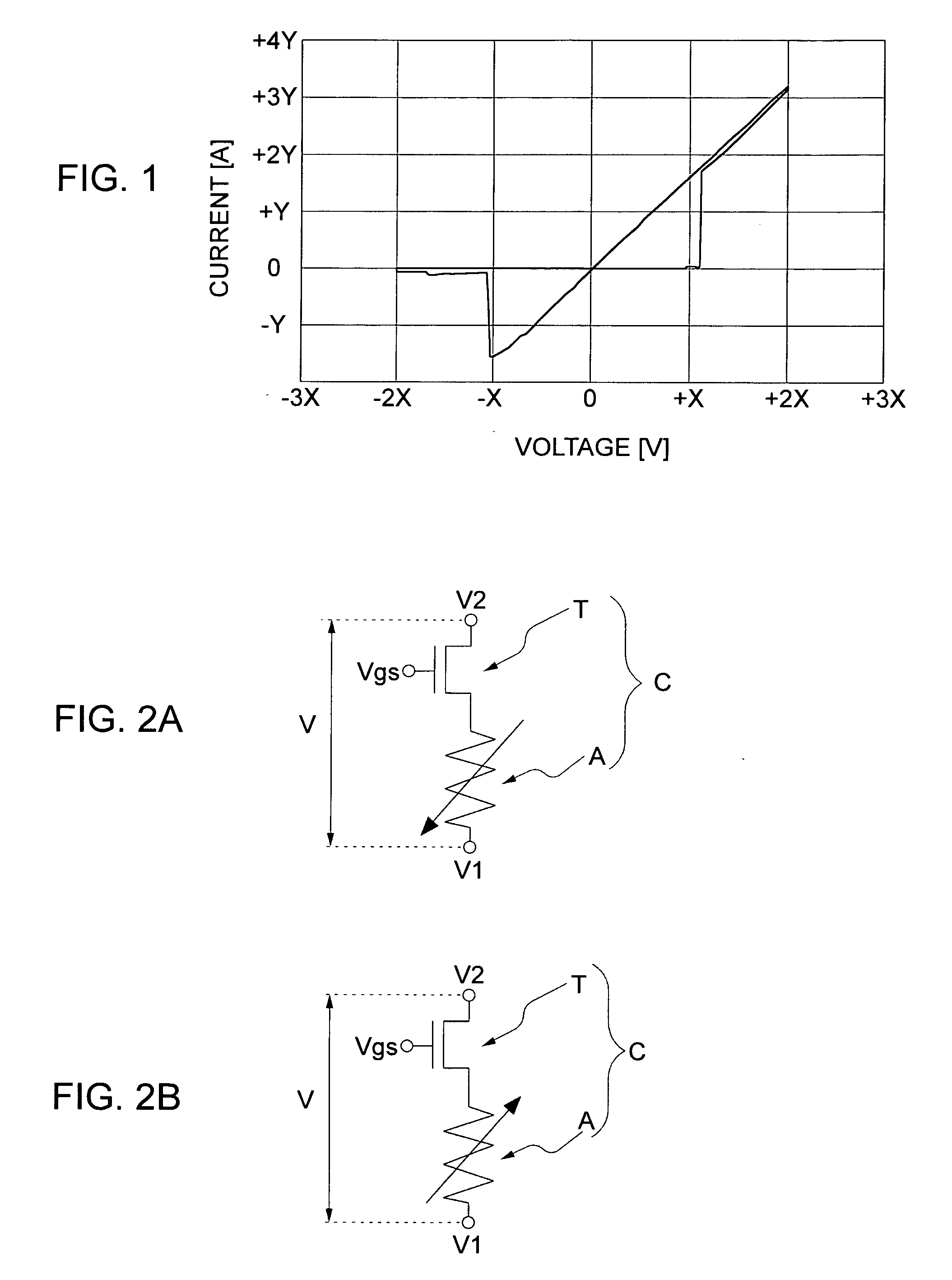
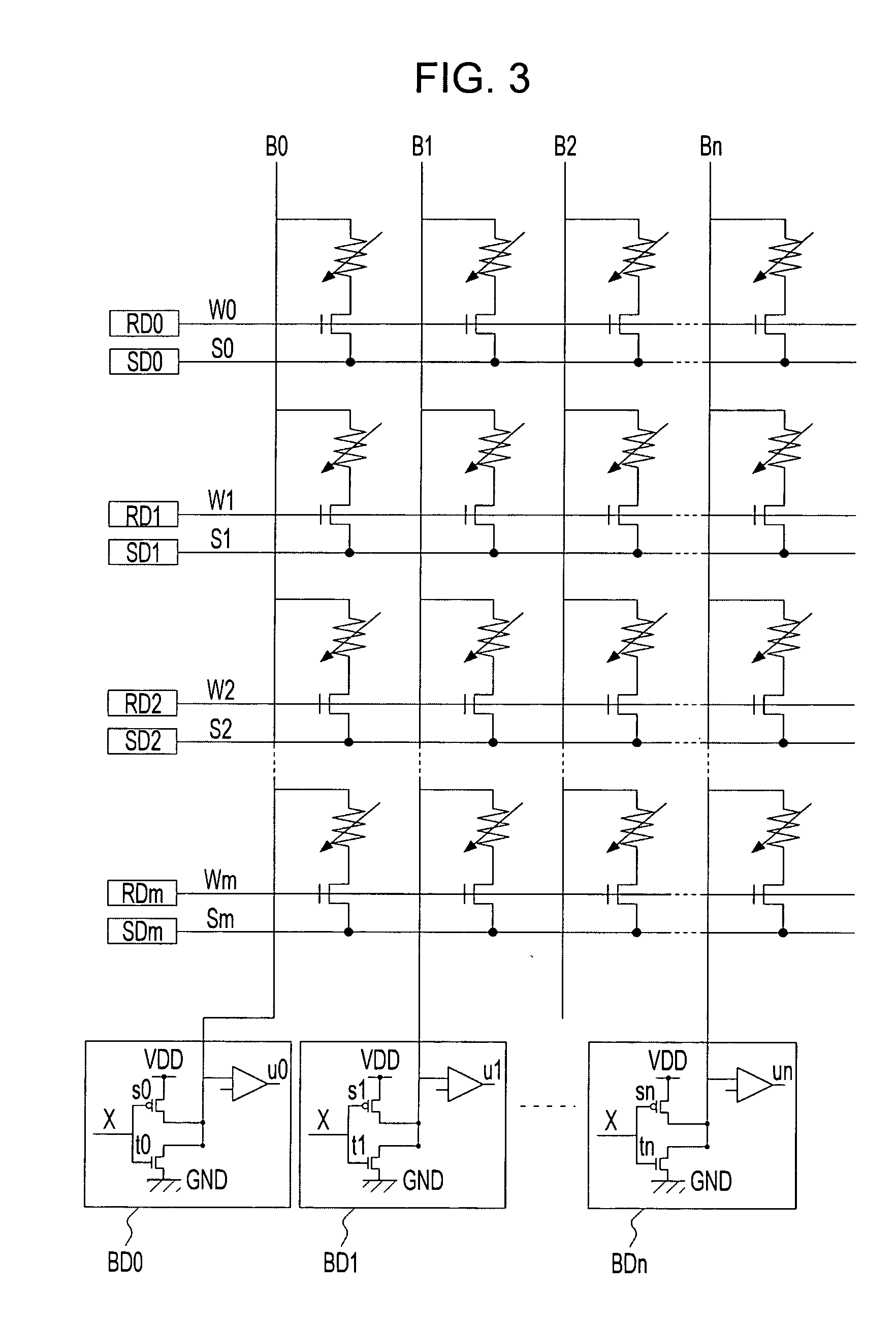
[0045] Embodiments of the present invention will be described below with reference to the drawings to provide an understanding of the present invention. In the following embodiments, a resistance change memory element (hereinafter, referred to a memory element) is used in each memory cell and a memory includes such memory cells.

[0046]FIG. 1 is a graph showing the current-voltage (I-V) characteristic of a memory element (1) used in a memory according to an embodiment of the present invention.

[0047] The memory element (1) having the I-V characteristic shown in FIG. 1 includes, e.g., a memory element including first and second electrodes (e.g., lower and upper electrodes) and a memory layer arranged between the first and second electrodes, the memory layer including an amorphous thin film, such as a rare-earth oxide film.

[0048] In the initial state of the memory element (1), the resistance thereof is large (e.g., 1 MΩ or higher), i.e., a current is difficult to flow therethrough. Wh...


PUM


Abstract

A memory includes: memory elements arranged in a matrix, each memory element having such characteristics that when an electric signal at a level equal to or higher than that of a first threshold signal is applied to the memory element, the resistance thereof is changed from a high value to a low value, and when an electric signal at a level equal to or higher than that of a second threshold signal is applied thereto, the resistance is changed from the low value to the high value, the polarities of the first and second threshold signals being different from each other; electric circuits for applying electric signals to the memory elements; and detection units each for measuring a current flowing through the corresponding memory element or a voltage applied thereto from the start of the application of electric signals to detect whether the resistance is high or low.

Description

CROSS REFERENCES TO RELATED APPLICATIONS [0001] The present invention contains subject matter related to Japanese Patent Application JP 2004-320503 filed in the Japanese Patent Office on Nov. 4, 2004, the entire contents of which are incorporated herein by reference. BACKGROUND OF THE INVENTION [0002] 1. Field of the Invention [0003] The present invention relates to memories and semiconductor devices and, more particularly, to a memory and a semiconductor device, which detect a state of each memory element during a write sequence or an erase sequence to reduce time necessary for writing or erasing. [0004] 2. Description of the Related Art [0005] In information equipment, such as computers, high-speed and high-density dynamic random access memories (DRAMs) are widely used as random access memories. [0006] The DRAM is volatile, i.e., it loses information when powered off. Accordingly, a nonvolatile memory which does not lose information when powered off is preferable. [0007] Up-and-co...

Claims


Application Information

Patent Timeline
Patent Type & Authority Applications(United States)
IPC IPC(8): G11C7/02H10B69/00
CPCG11C13/004G11C13/0064G11C13/0069G11C2013/0054G11C2213/79G11C11/21
Inventor HACHINO, HIDENARIMORI, HIRONOBUOKAZAKI, NOBUMICHIARATANI, KATSUHISA
Owner SONY CORP
Why Eureka
Try Eureka