
ASICs having more features than generally usable at one time and methods of use

a technology of integrated circuits and features, applied in logic circuits using specific components, pulse techniques, instruments, etc., can solve the problems of low efficiency, low efficiency, and low efficiency of standard cells, so as to reduce the cost of lithographic fabrication, design, and other design related costs of the ic, and reduce the time to market. , the effect of reducing the cost of per di

Active Publication Date: 2006-04-13
SHEYU GROUP
View PDF5 Cites 29 Cited by
  • Summary
  • Abstract
  • Description
  • Claims
  • Application Information

AI Technical Summary

Benefits of technology

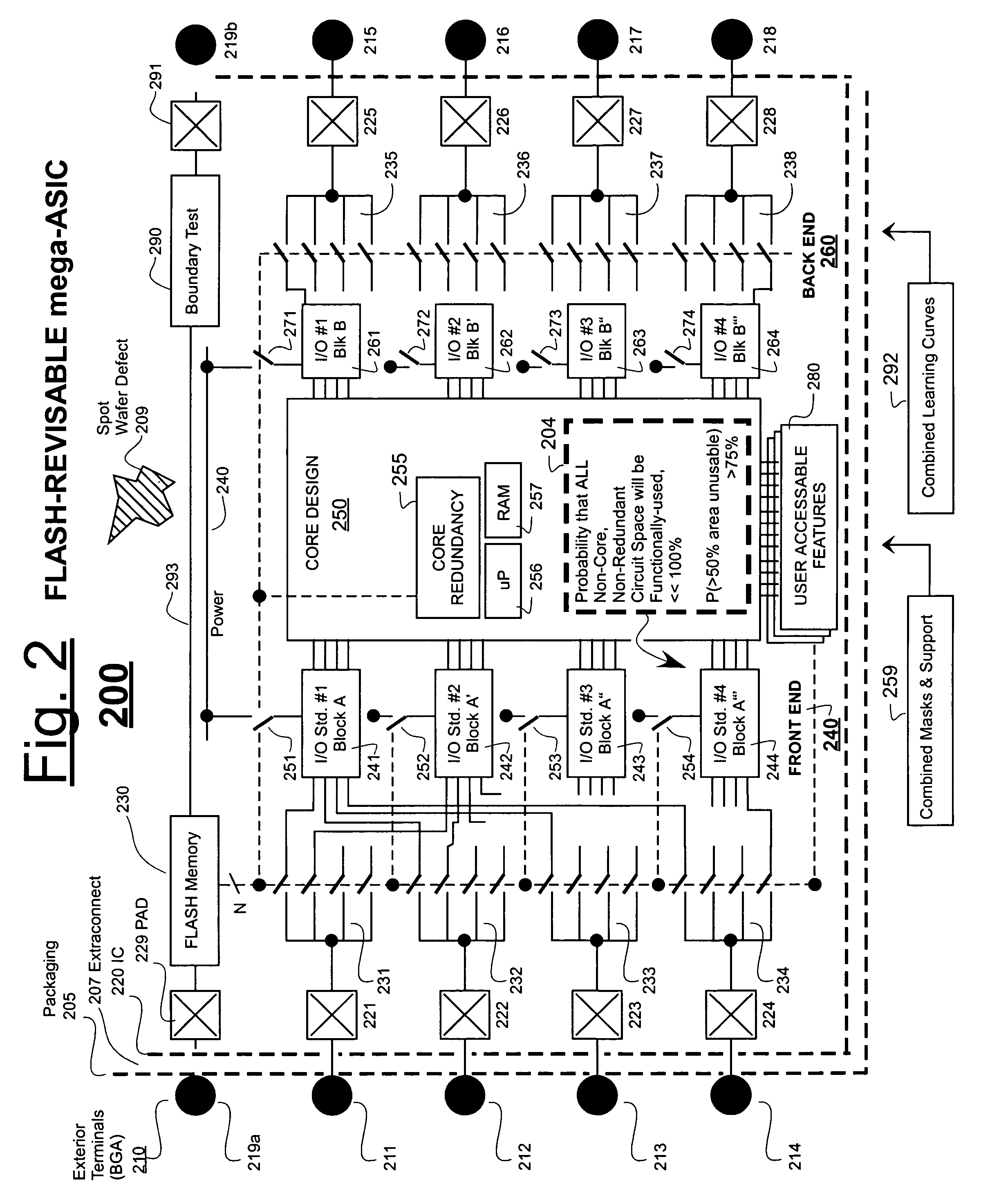
[0014] Despite these apparent or real drawbacks, there are advantages which can more than offset the drawbacks. First, when consumer demand suddenly shifts toward demanding a new mix of features, time to market can be significantly reduced if some of the over-abundant but included functionalities of the already-mass-produced and on hand mega-ASIC's happen to meet the new and emerging market demands. The surplus functionality may be programmably activated to quickly meet the newly emerging market demands without having to wait for redesign, tape-out and special-run fabrications. Second, the per-die costs for supporting lithographic fabrication, design, and other design related costs of the IC can be reduced if a single set of photolithography masks (or other patterning means) and / or a single manufacturing plant (foundry) can be used to support different market spaces such as different regions around the world (e.g., Japan, Europe, USA, China—each of which regions often tends to have a unique mix of interoperability standards of its own). Gains from the manufacturing learning curve of one version of the common IC can apply to the manufacture of alternately activated versions of the same IC, where those alternately activated versions are to be used in different parts of the world or to service different market demographics (e.g., young students versus senior citizens).

Problems solved by technology

It is desirable to use a relatively minimal number of building blocks because IC circuit space is considered expensive.
This form of optimization is not perfect though because specific ones of the general purpose applications may nonetheless call for different switching speeds, frequency ranges, voltages, currents and fabrication technologies.
So a standard cell is rarely the most optimally compact and efficient design for a specific application.
One outstanding disadvantage of using standard cells is that there is little room for flexibility and design change after specific ones of the hardwired cells have been chosen, judiciously inserted into the ASIC design and stitched together.
By contrast, consumer markets tend to be very fluid and fickle.
This is a very dangerous situation for ASIC manufacturers and marketing managers.
A warehouse full of what, on one day is highly-demanded product, can become worthless overnight as the winds of consumer demand shift directions.
However, after the ASIC is put into mass production, market forces are such that the majority of customers change their minds and decide they want product that instead uses a different and incompatible, input processing protocol say, decompression algorithm B. A popular journalist may have indicated he likes B better and suddenly consumers are demanding products that use decompression algorithm B. In such a case, the mass-produced ASIC's which the designer has in his warehouses become essentially un-saleable.
The marketing manager failed to accurately predict the hard-to-predict changes in future market trends, where the future is one or two years ahead of time, the time required to design and mass produce an IC chip under current technology constraints.
As a result, his company is not able to sell more than a few of the algorithm A chips to what few customers are using algorithm A. Often, so-called network effects for interoperable devices are at work.
The problem with the field-programmable approach, however, is that the fully-programmable circuitry tends to be more expensive, larger in size, slower in response time and prone to various problems which ASIC circuitry does not generally suffer from.
One sample problem is that of having flawed software loaded into one or more of the many configuration memory cells (or fuses or anti-fuses) of a field-programmable device.
Then the fully programmable device fails to work properly just because of the flaw.
This disclosure challenges that fundamental belief.
One clear disadvantage of mass producing such a mega-ASIC, in other words, an IC that is excessively crammed with hardwired functionality where a non-negligible portion of the IC's precious circuit space will definitely (or with high probability) be wasted in a given market space, is that this increases the cost of providing the useable functionality in the remaining parts of the IC.
Another disadvantage is that fewer dice will be produced from each mass produced wafer that contains such surplus-containing IC dice.
Yet another disadvantage which appears to flow from such mass production of such overly-large dice is the reduction of yield since it is conventionally accepted that yield decreases with increase in die size.

Method used


Image

  • ASICs having more features than generally usable at one time and methods of use
  • ASICs having more features than generally usable at one time and methods of use
  • ASICs having more features than generally usable at one time and methods of use

Examples


Embodiment Construction

[0021]FIG. 1 is a block diagram illustrating a hypothetical situation 100 to which the here disclosed invention may be applied. It is assumed that industry standardizing committees have devised a roadmap for a new type and emerging of technology called Dynamic-Resolution Ultra-High Definition Television (DR-UHDTV). The specifics of what technologies might constitute DR-UHDTV is unimportant here. It is a hypothetical example. What is important here is that an intermediary product 102 will be developed that, among other things, will support interoperability with other DR-UHDTV-related devices (e.g., 106, 107, 108) according to locally adopted, interoperability standards. Assume for example that first signals 101a represent DR-UHDTV programming content that is to be stored in some form of data storage disk cartridge 106 in, for example, DVD or VCD or SVCD format depending on different regions of use and that second signals 101b represent DR-UHDTV programming content that is to be trans...


PUM


Abstract

More ASIC functionality is crammed into a chip (or chip set) than can probably or definitely be operative at one time when the chip is packaged and inserted into a broader circuit. The excessive ASIC functionality is chosen to cope with different market development probabilities in a host of different market spaces (e.g., in different countries where different interoperability standards are chosen) and a subset of the excessive ASIC functionality is programmably activated in each market space after manufacture. Customer behavior can be fickle. If market trends evolve towards demand for functionality #2 instead of an originally, more expected, functionality #1, the mass produced of the crammed chip (or chip set) is not out of necessarily out of luck. If the mass produced had enough foresight to cram in functionality #2 as well as functionality #1, the producer can programmably activate #2, and deactivate #1 as market demand suddenly shifts in a given market space. In one embodiment, a mega-ASIC with excessive ASIC functionality crammed into it, has a universal core as well as plurality of programmably selectable ASIC function blocks. The ASIC function blocks are programmably activatable and de-activatable so that a mass produced can quickly respond to shifting market demands, thus addresses both time to market and product life issues. The invention allows a small chip designer to simultaneously address more than one market or customer space with one ASIC chip thereby reducing the design cost per product design. By selectively activating the excessive and selectable ASIC functionalities, the small ASIC chip designer can appear to sport different features for different customers and different markets at different times with just one chip, thus he can aggregate the demand of different customers and different markets to achieve economies of scale, and of inventory management and control.

Description

FIELD OF DISCLOSURE [0001] The present invention relates generally to Application Specific Integrated Circuits (ASIC's) and more specifically to the marketing of, design of, manufacture of and distribution of ASIC's for use in different consumer markets. DESCRIPTION OF RELATED ART [0002] Low cost electronic products that are sold to mass consumer markets often include ASIC's (Application Specific Integrated Circuits). Conventional ASIC methodology relies on libraries of so-called, “standard cells”. These libraries contain large numbers of pre-designed circuits (basic building blocks). When a new consumer product is designed to include one or more ASIC's, a subset of the pre-designed cells are typically chosen from available libraries for inclusion in the operative circuit space of the to-be-manufactured, monolithic integrated circuit (IC) and for use in a predefined consumer application (e.g., cell phone, PDA, video / music recorder / player, etc.). After the subset of cells are selecte...

Claims


Application Information

Patent Timeline
IPC IPC(8): G06F17/50H03K19/00
CPCG06F17/5045G06F30/30
Inventor KOO, JAMES T.
Owner SHEYU GROUP
Learn More