
Single chip stereo imaging system with dual array design

Inactive Publication Date: 2006-04-13
DIGITAL IMAGING SYST
View PDF13 Cites 21 Cited by
  • Summary
  • Abstract
  • Description
  • Claims
  • Application Information

AI Technical Summary

Benefits of technology

[0013] It is also still further an objective of the present invention to place two light sensitive arrays within a single reticule of a semiconductor process to produce circuit elements without the need to stitch together different portions of the circuitry that forms the chip.
[0015] An optical unit comprising two lenses, a left lens and a right lens, is used to focus distant objects onto the two imaging arrays, a left imaging array and a right imaging array. A single optical substrate containing the two lenses is positioned between the imaging chip and distant objects to focus the distant objects onto the imaging arrays. The left lens focuses a first image of the distant objects onto the left imaging array, and the right lens focuses a second image of the distant objects onto the right imaging array. The material of the optical substrate is chosen to have a temperature coefficient as close to that of the semiconductor substrate as possible to minimize alignment tolerances over a temperature range and maximize the accuracy of the computational comparison of the two images in, for example, a computation of the distance from the stereo imaging system and distant objects.

Problems solved by technology

These imaging systems usually require a critical alignment of elements of the system and stability over a range of temperature is hard to control.
Some of the imaging systems have complex optics requiring a critical alignment of the optics and the cameras that capture the images.
In all cases the positioning of individual parts of the system have distances with tolerances that are difficult to control, and especially with respect to temperature variations of the system.

Method used


Image

  • Single chip stereo imaging system with dual array design
  • Single chip stereo imaging system with dual array design
  • Single chip stereo imaging system with dual array design

Examples


Embodiment Construction

[0023] In FIG. 2 is shown a plan view of a semiconductor device 20, which contains two imaging arrays, a left imaging array 21L and a right imaging array 21R. The two imaging arrays are located at opposite edges the semiconductor device 20 with the left imaging array 21L located near the left edge of the device and the right imaging array 21R located near the right edge of the device. Support circuitry and a computational unit occupy the area 22, which is not occupied by the two imaging arrays 21L and 21R. The support circuitry comprises, a clock, regulators, analog signal chains, analog to digital converters and a FPGA. The computational unit is either a DSP or a computational unit created from synthesized logic.

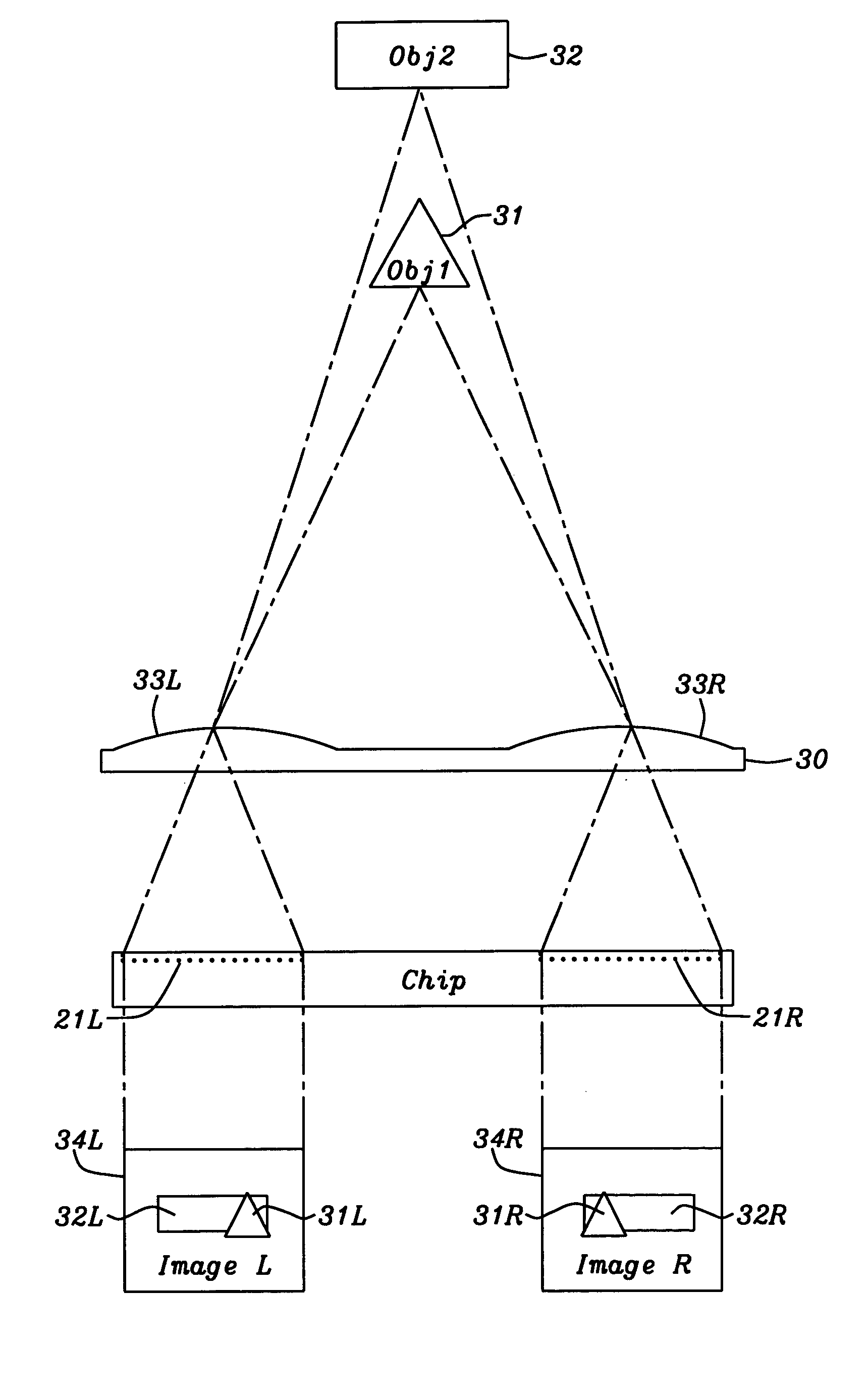
[0024] In FIG. 3 is a diagram of the present invention showing the stereo imaging chip 20, a focusing unit 30 and two distant objects Obj131 and Obj232. On the semiconductor imaging device 20 are located a left imaging array 21L and a right imaging array 21R. The focusing ...


PUM


Abstract

A stereo imaging chip is presented that contains two imaging arrays located at opposite edges of the chip. Support circuitry, including a computational unit, is located on the chip in areas not occupied by the imaging arrays. A FPGA located on the chip is used to provide instructions to the computational unit and allow updates. A stereo focusing unit on a single optical substrate focuses a distant object onto the two imaging arrays. The semiconductor process producing the chip provides accurate alignment of the two imaging arrays and the use of a single optical substrate to containing the stereo lens provides additional dimensional accuracy and stability to allow calculations of the distance to distant objects.

Description

BACKGROUND OF THE INVENTION [0001] 1. Field of Invention [0002] The present invention relates to semiconductor imaging chips and in particular to a single CMOS chip with two imaging arrays to form a stereo imaging device. [0003] 2. Description of Related Art [0004] There are several configurations that have been developed to capture stereo images using two physical cameras, or a single camera with a prism system to deliver a stereo image to the single camera. Systems containing both video cameras and still cameras have been developed, but each camera only contains a single imaging device. Besides the requirement to create three-dimensional (3-D) images, an additional use of stereo imaging systems is to measure distance to objects remote from the system. These imaging systems usually require a critical alignment of elements of the system and stability over a range of temperature is hard to control. [0005] In U.S. Pat. No. 6,611,664 B2 (Kochi et al.) a system is directed to a stereo i...

Claims


Application Information

Patent Timeline
IPC IPC(8): H01L27/00H04N13/239
CPCH04N13/0239H04N13/239
Inventor DOSLUOGLU, TANERFRIEDEL, JURGEN
Owner DIGITAL IMAGING SYST
Learn More