
Nonvolatile memory apparatus

a memory apparatus and non-volatile technology, applied in the direction of static storage, digital storage, instruments, etc., can solve the problems of overhead latency time taken during the operation for reading from the memory array to the data buffer, and the inability to output data in the data buffer corresponding to each inactive bank to the outside, so as to achieve the effect of greatly improving the output at reading high-volume data

Inactive Publication Date: 2006-02-02
RENESAS TECH CORP
View PDF9 Cites 24 Cited by
  • Summary
  • Abstract
  • Description
  • Claims
  • Application Information

AI Technical Summary

Benefits of technology

[0010] These occurred because upon comparison between the write operation and the read operation of the nonvolatile memory, the read operation was relatively faster than the write operation, and there was less demand for a reduction in temporal overhead taken for the operation of reading from the memory array to the data buffer.
[0011] Therefore, an object of the present invention is to provide a technique capable of, in a nonvolatile memory apparatus having a plural-bank configuration, reducing the above overhead and improving throughput at reading of high-volume data.
[0018] Since only a first access time is visible to the outside where a read command is issued continuously plural times, throughput at reading of high-volume data can be greatly improved.

Problems solved by technology

That is, while the operation for reading from the memory array to the data buffer was in execution, it was not possible to input the next command and output data lying in the data buffer to the outside.
While there was a bank executing the operation for reading from a memory array to its corresponding data buffer, it was not possible to output data in a data buffer corresponding to each inactive bank to the outside.
Therefore, a latency time taken during the operation for reading from the memory array to the data buffer became overhead at reading of high-volume data.

Method used


Image

  • Nonvolatile memory apparatus
  • Nonvolatile memory apparatus
  • Nonvolatile memory apparatus

Examples


Embodiment Construction

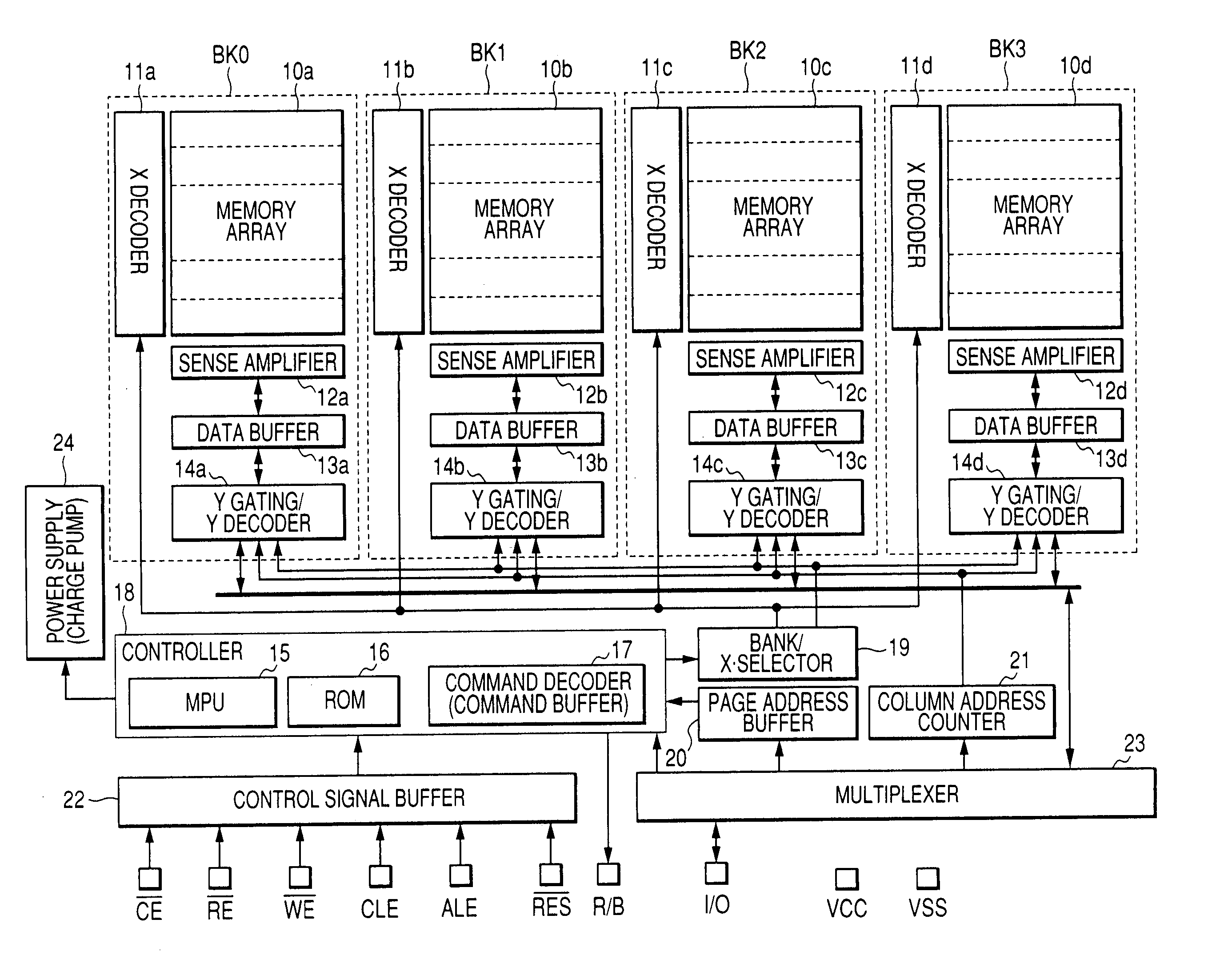
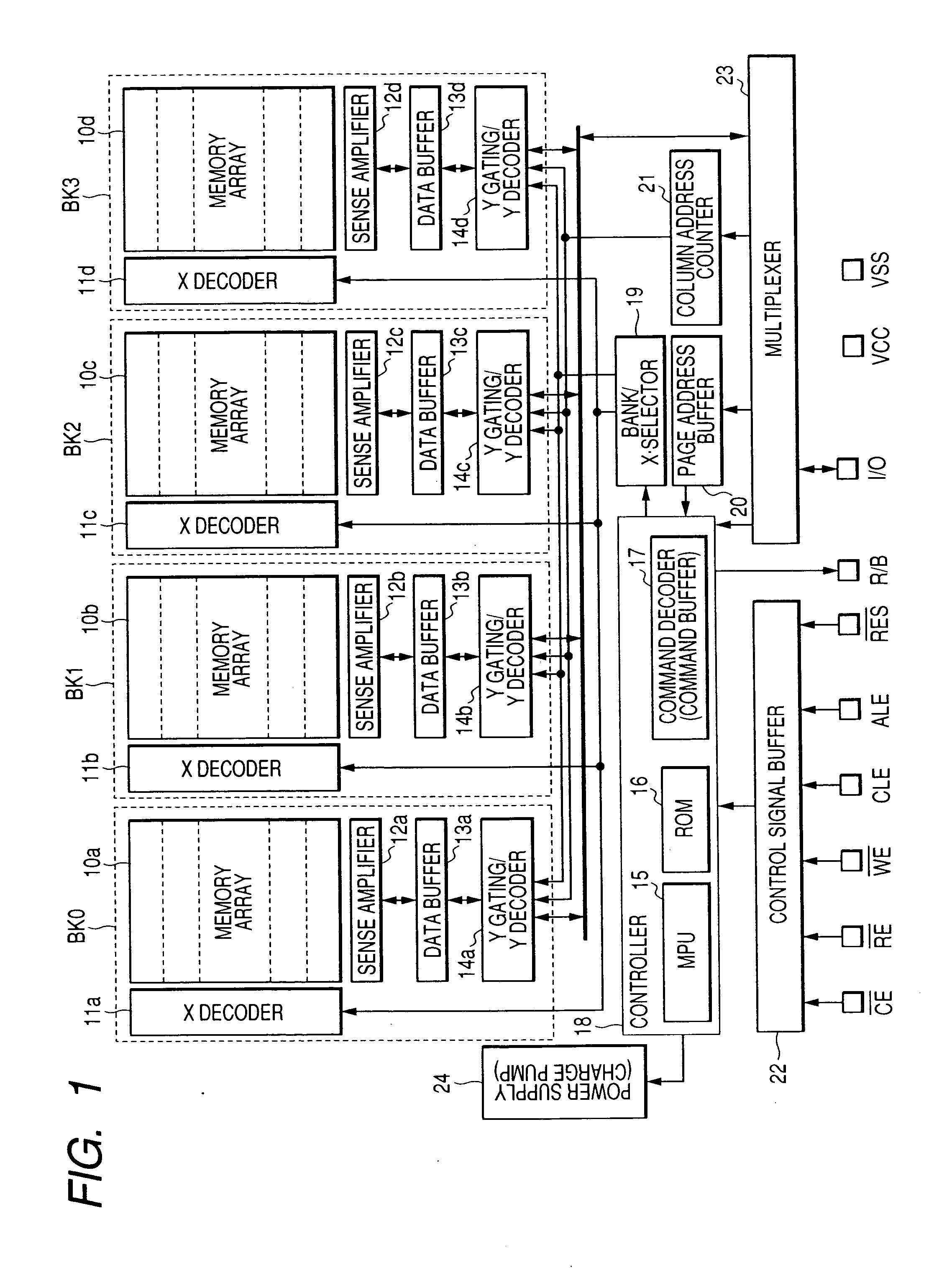
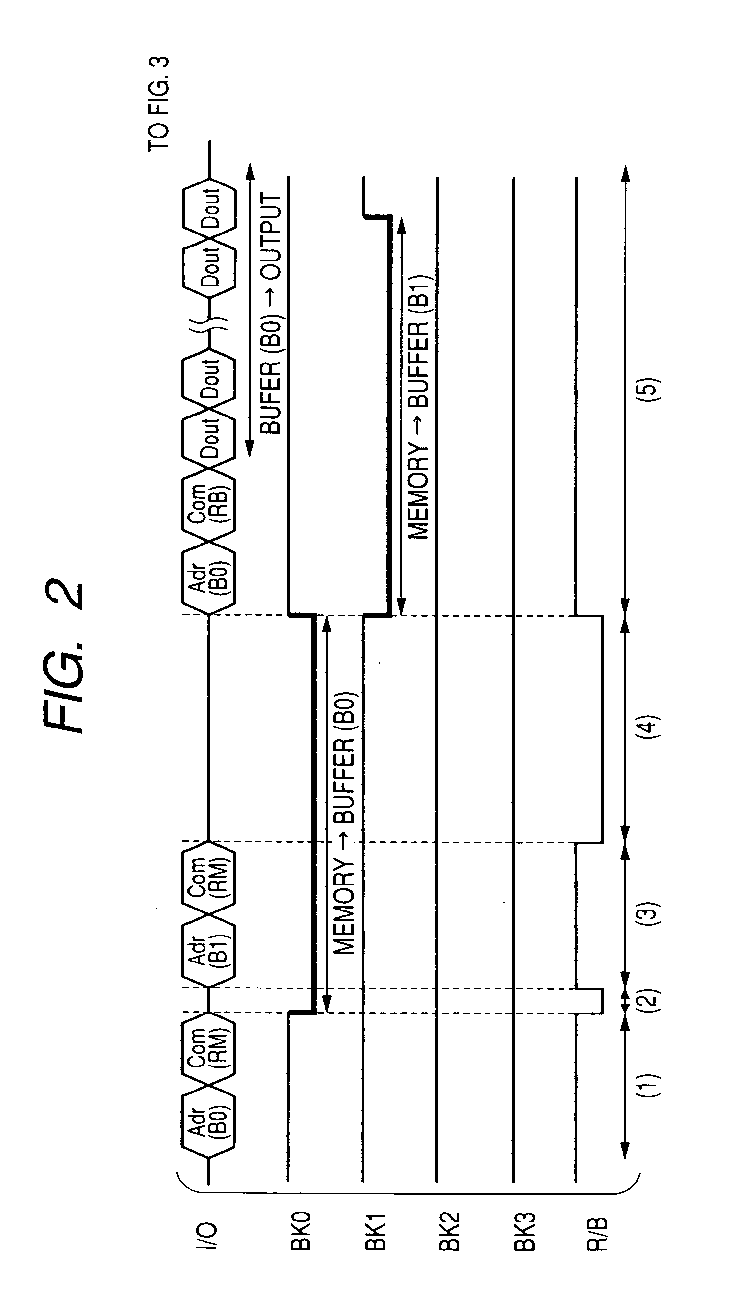
[0034] Preferred embodiments of the present invention will hereinafter be described in detail with reference to the accompanying drawings. Incidentally, the same components or members are given the same reference numerals in principle in all the drawings for describing the preferred embodiments, and their repetitive explanations are therefore omitted.

[0035]FIG. 1 is a block diagram showing a configuration of a nonvolatile memory apparatus according to one embodiment of the present invention, FIGS. 2 through 4 are respectively timing charts each showing a one-page cache read operation at a one-stage command buffer in the nonvolatile memory apparatus according to the present embodiment, FIG. 5 is a timing chart showing a one-page cache read end operation, FIGS. 6 through 9 are respectively timing charts each showing a two-page cache read operation at a one-stage command buffer, FIG. 10 is a timing chart showing a two-page cache read end operation, FIGS. 11 through 12 are respectively...


PUM


Abstract

A read command having designated a bank, can be inputted from outside. A read command having designated a bank can be inputted from outside while an operation for reading from a memory array to a data buffer is being performed at the bank. Further, a read command having designated a bank is inputted from outside, and a buffer read command having designated a bank is inputted from outside while an operation for reading from a memory array to a data buffer is being performed at the bank, whereby reading from the data buffer of the bank to the outside is enabled.

Description

CROSS-REFERENCE TO RELATED APPLICATION [0001] The present application claims priority from Japanese patent application No. 2004-223077 filed on Jul. 30, 2004, the content of which is hereby incorporated by reference into this application. BACKGROUND OF THE INVENTION [0002] The present invention relates to a semiconductor memory device and a nonvolatile memory apparatus, and particularly to a technique effective if applied to a nonvolatile memory apparatus such as a nonvolatile memory having a plural-bank configuration. [0003] As a technique discussed by the present inventors, there is known one like a nonvolatile memory such as a flash memory or the like, wherein memory arrays each including a plurality of memory cells are divided into a plurality of banks, which are respectively equipped with decoders, data buffers, etc., and memory operations such as erasure, writing, reading, etc. are performed independently every banks. There are known various techniques for improving throughput...

Claims


Application Information

Patent Timeline
Patent Type & Authority Applications(United States)
IPC IPC(8): G11C8/00
CPCG11C2216/22G11C16/32G11C16/02
Inventor MATSUSHITA, TORUKOZAKAI, KENJITANABE, HAJIMEHORII, TAKASHI
Owner RENESAS TECH CORP
Learn More