Control circuit of DC-DC converter and its control method
- Summary
- Abstract
- Description
- Claims
- Application Information
AI Technical Summary
Benefits of technology
Problems solved by technology
Method used
Image
Examples
first embodiment
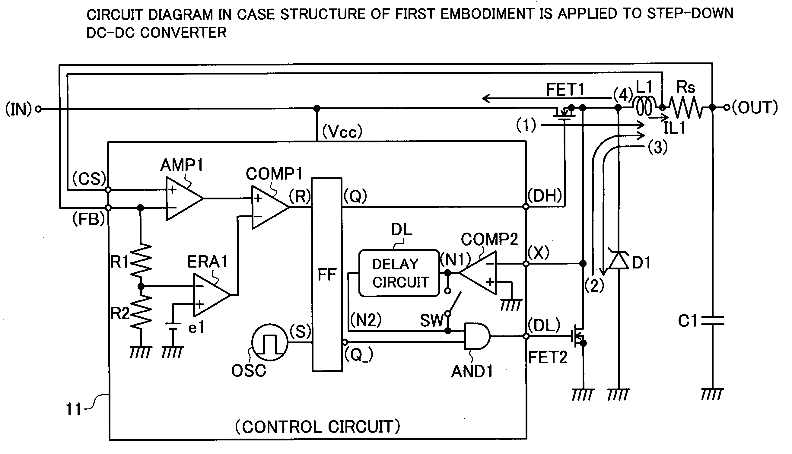
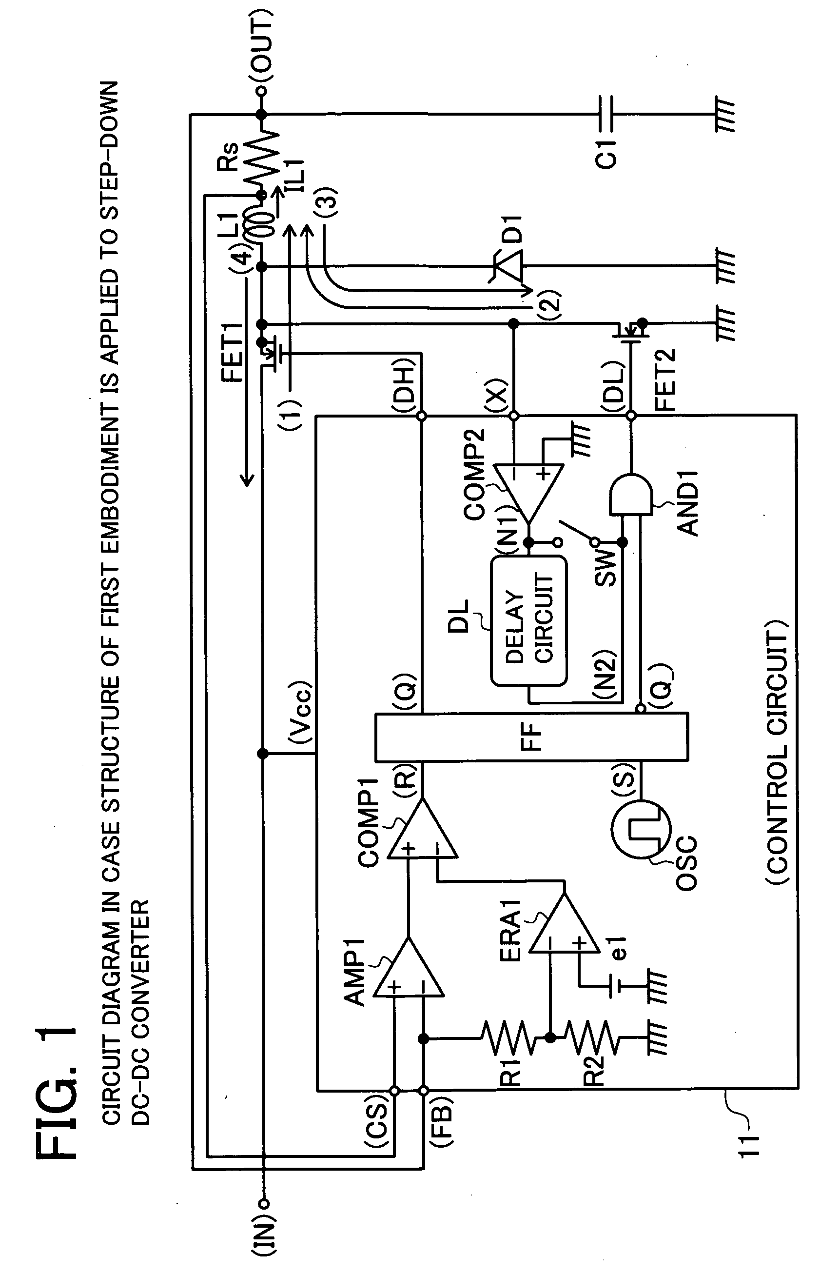
[0047]FIG. 1 is a circuit diagram of a first embodiment applied in a step-down DC-DC converter. The non-conductive timing of synchronous transistor which conducts when discharging an electric power to the load is delayed from the zero timing of discharge current toward the load after completion of power discharge. For the delayed period, the synchronous transistor is maintained in conductive state, and the discharge current is inverted, and the load side excess power is returned.
[0048] An input terminal (IN) in which input voltage VIN is supplied is connected to a drain terminal of NMOS transistor FET1. A source terminal of the NMOS transistor FET1 is connected to one terminal of choke coil L1 and a drain terminal of NMOS transistor FET2. A source terminal of the NMOS transistor FET2 is connected to a grounding potential. Gate terminals of the NMOS transistors FET1, FET2 are respectively connected to output terminals (DH), (DL) of a control circuit 11 which is described later. A dio...
second embodiment
[0078]FIG. 4 is a circuit diagram of a second embodiment applied in a step-down DC-DC converter. The non-conductive timing of synchronous transistor conducting when discharging electric power to the load can be set as the timing of returning the load side excess power by inversion of the discharge current by setting offset in the detection of discharge current. By addition of offset, the non-conductive transition of synchronous transistor is delayed, and the load side excess power is returned.
[0079] In a control circuit 12 shown in FIG. 4, instead of the switch circuit SW and delay circuit DL in the control circuit 11 in FIG. 1, switch circuit SW2 and offset unit e2 are provided. At the input terminal of the AND gate circuit AND1, an output terminal of comparator COMP2 is connected instead of output terminal (N2) of delay circuit DL. Other circuit configuration is same as in FIG. 1, and the explanation is omitted.
[0080] The switch circuit SW2 connects either grounding potential or ...
third embodiment
[0084]FIG. 5 is a circuit diagram of a third embodiment applied in a step-down DC-DC converter. In a DC-DC converter capable of selecting the PWM fixed control and PWM / PFM variable control, the conduction control of synchronous transistor is made non-conductive by preventing counterflow of coil current by having rectifying action in the PWM / PFM variable control, and the counterflow of coil current is permitted and conductive state is maintained in the PWM fixed control. In the PWM fixed control for supplying power to the load side in every period, it is composed to return the load side excess power in every period.
[0085] In a control circuit 13 shown in FIG. 5, instead of the switch circuit SW and delay circuit DL in the control circuit 11 in FIG. 1, an OR gate circuit OR1 is provided. An input terminal of OR gate circuit OR1 is connected to an output terminal of comparator COMP2, and receives selection signal DSA of PWM fixed control. The selection signal DSA is a signal which is h...
PUM
 Abstract
Description
Claims
Application Information
 - R&D
- Intellectual Property
- Life Sciences
- Materials
- Tech Scout
- Unparalleled Data Quality
- Higher Quality Content
- 60% Fewer Hallucinations
Browse by: Latest US Patents, China's latest patents, Technical Efficacy Thesaurus, Application Domain, Technology Topic, Popular Technical Reports.
© 2025 PatSnap. All rights reserved.Legal|Privacy policy|Modern Slavery Act Transparency Statement|Sitemap|About US| Contact US: help@patsnap.com


