
External storage device

Inactive Publication Date: 2005-12-22
BUFFALO CORP LTD
View PDF4 Cites 84 Cited by
  • Summary
  • Abstract
  • Description
  • Claims
  • Application Information

AI Technical Summary

Benefits of technology

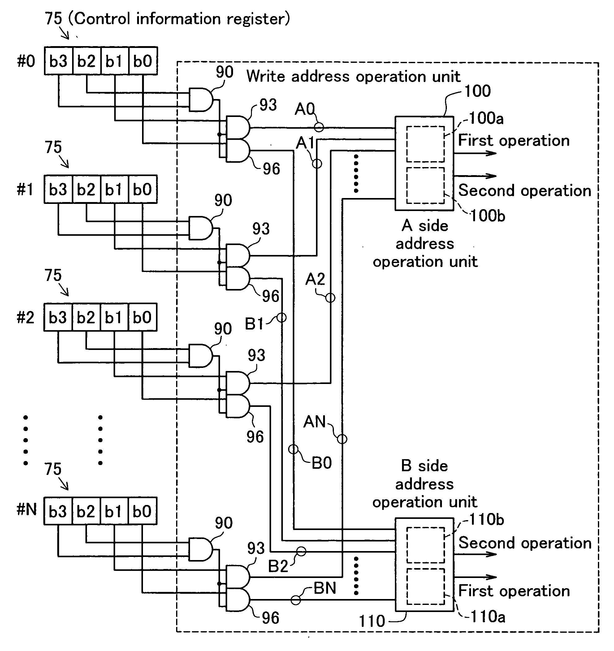
[0011] According to the aspect of the external storage device and the method thereof of the present invention, based on the use status and the erase count information stored in each block constituting the flash memory, the plurality of blocks is classified into n groups according to the erase count. During data write, the usable (in other words, empty) blocks of one of the classified groups are used in the block constitution sequence. When all of the empty blocks of one group are used, the data is written to the usable blocks of another group selected in a specified sequence. Between the sequential n groups, the items in charge for selecting the block used for data write are alternated, and data is written to the selected block. Therefore, by the n groups classified according to the erase count being sequentially alternated, it is possible to level the block erase count as the overall flash memory. Also, the process of selecting the block used for external storage device data write is constituted using hardware circuits including registers or gates, so it is possible to increase the processing speed compared to processing using software.
[0013] According to this aspect of the external storage device, the usable blocks are classified into two groups, the groups for which the erase count is 0 times or an even number of times, and the odd numbered groups, and the item in charge for selecting the block used for writing is repeatedly alternated between both groups. Therefore, it is possible to easily construct a system using a few registers and gates.
[0016] According to this external storage device, at the write timing of data to one block, the logical address of that written data is stored in the logical address register. When reading data from the flash memory, the logical address for which reading is desired and the address stored in the logical address register of all the blocks being used are compared by each comparator at once. As a result of comparison, the desired data is output from the concerned block. Therefore, no matter which block within the flash memory the specified data is stored in, it is possible to execute reading of the desired data instantly by using each comparator.
[0017] The storage means of the external storage device having the constitution noted above may also be means that generate a table for representing the corresponding relationship between the logical address that is the address on the virtual memory space allocated as the storage area of the data and the physical address of the block selected by the block selection means and in which the data is stored, and that store the data based on this table. According to this external storage device, selection of the usable blocks is performed using hardware, and the table for representing the corresponding relationship is generated using software. By using this table, it is possible to easily select the physical address corresponding to the logical address, and to read the desired data.

Problems solved by technology

On the other hand, flash memory has structural limitations such as that data erasing is performed in block units, and that the number of block erases is limited.
Specifically, by repeating erasing only of specific blocks, there is a marked decrease in life as memory.
However, with this kind of address conversion process, complex firmware software is required for converting the logical address and the physical address, and manufacturing of the firmware was complex and also took time for processing.
Also, when this kind of process is executed using software, the processing by software increases, so in fact, significant time is used for processing.

Method used


Image

  • External storage device
  • External storage device
  • External storage device

Examples


Embodiment Construction

[0035] Following, aspects of implementing the present invention are described based on embodiments in the following order. [0036] A. Schematic Structure of External Storage Device: [0037] B. Write Block Leveling Process: [0038] (B-1) First Operation Circuit: [0039] (B-2) Second Operation Circuit: [0040] (B-3) Block Identification Circuit: [0041] (B-4) Example of Leveling Circuit: [0042] C. Data Access Processing: [0043] D. Variation Examples:

A. SCHEMATIC STRUCTURE OF EXTERNAL STORAGE DEVICE

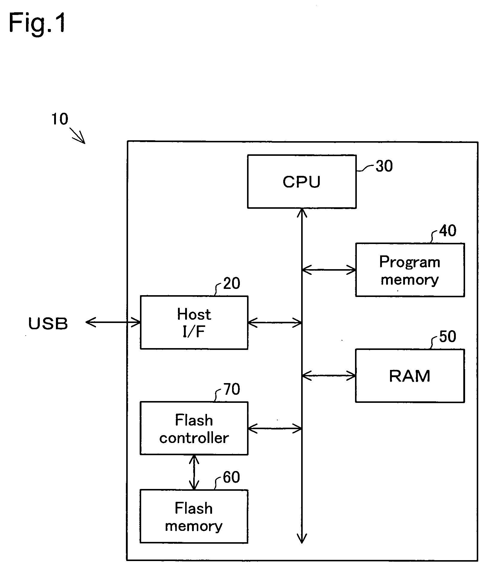
[0044]FIG. 1 is an overall block diagram showing the constitution of the external storage device 10 as the first embodiment of the present invention. As shown in the drawing, this external storage device 10 comprises a host interface 210 for exchange data with external devices, a CPU 30, a program memory 40, a RAM 50, a flash memory 60 for doing non-volatile storage of data from outside, a flash controller 70 for controlling reading of data to the flash memory 60, and the like.

[0045] The host i...


PUM


Abstract

By providing registers for each block constituting the flash memory, based on the use state and the erase count information stored in the registers, the plurality of blocks are classified into n groups according to the erase count by the control circuit, and of the blocks that can be used for writing of one classified group, writing of data is performed in the block constitution sequence. When all the blocks of one group are used, data is written to blocks that can be used for writing of another group selected in a specified sequence. Sequentially between n groups, the item in charge for selecting the blocks used for data writing are alternated, and data is written to the selected block. As a result, considering leveling of the flash memory block erase count, it is possible to perform the write capability block selection process using hardware.

Description

CLAIM OF PRIORITY [0001] The present application claims priority from Japanese application P2004-4097 filed on Jan. 9, 2004, the content of which is hereby incorporated by reference into this application. BACKGROUND OF THE INVENTION [0002] 1. Field of the Invention [0003] The present invention relates to an external storage device that incorporates flash memory. [0004] 2. Description of the Related Art [0005] From the past, there have been external storage devices that incorporate flash memory which is non-volatile semiconductor memory. With flash memory, data does not disappear even when the power is shut off, and it has features such as that it has a comparatively low price compared to EEPROM (Electrically Erasable Programmable ROM) which is another non-volatile memory. On the other hand, flash memory has structural limitations such as that data erasing is performed in block units, and that the number of block erases is limited. Specifically, by repeating erasing only of specific ...

Claims


Application Information

Patent Timeline
IPC IPC(8): G06F12/00G06F12/16G06F12/02G11C16/04G11C16/34G11C29/00
CPCG06F12/0246G06F2212/1036G11C29/76G11C16/349G06F2212/7211
Inventor ISHIDOSHIRO, TAKASHISONOBE, YOSHIIKU
Owner BUFFALO CORP LTD
Learn More