Display device and electronic device utilizing the same
a display device and electronic device technology, applied in non-linear optics, instruments, optics, etc., can solve the problems of limited size or brightness of conventional lcds with dual display panels, and achieve the effect of equal resolution quality and better brightness
- Summary
- Abstract
- Description
- Claims
- Application Information
AI Technical Summary
Benefits of technology
Problems solved by technology
Method used
Image
Examples
first embodiment
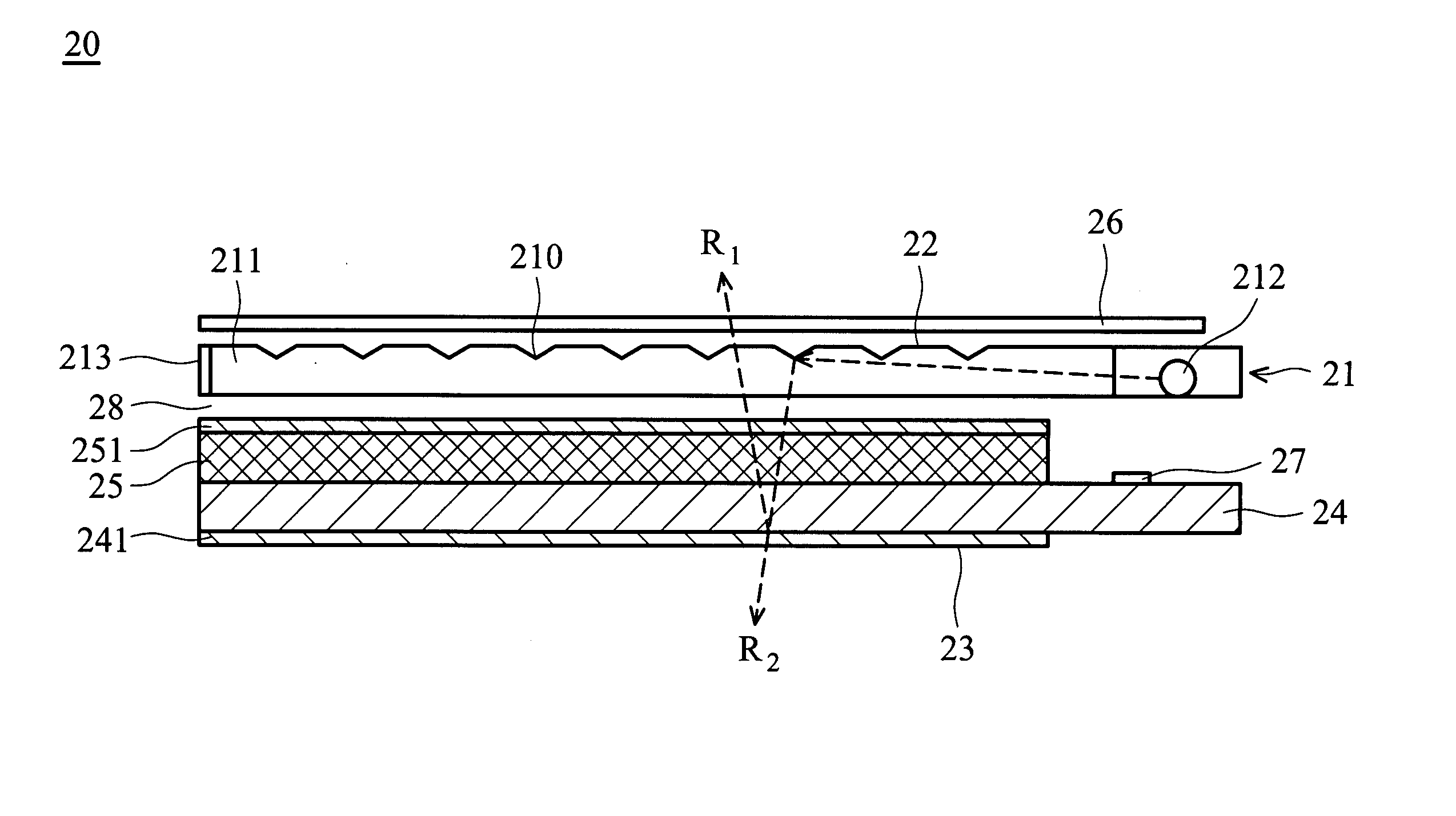
[0035]FIG. 2B is a cross section of a liquid crystal display 20 of the mobile phone 100 according to the first embodiment of the present invention. As shown in FIGS. 2A and 2B, the viewable screen of the liquid crystal display when the cover of the mobile phone 100 is closed is referred to as the first display side 22. The liquid crystal display 20 comprises a front light unit 21, a color filter 25, and a transmissive TFT panel 24. The color filter 25 is disposed under the front light unit 21 and above the TFT panel 24 with a gap 28 between the front light unit 21 and the color filter 25. The gap 28 having a thickness of about 0.1 mm provides clearance for preventing direct contact to the color filter 25. The transmissive TFT panel 24 has a second display side 23. An integrated circuit (IC) chip 27 is disposed on the TFT panel 24.
[0036] The front light unit 21 comprises a lamp 212, a light guide plate 211, a plurality of prism grooves 210, and a reflector 213. The lamp 212 disposed...
second embodiment
[0044]FIG. 3A is a cross section of a liquid crystal display 20 according to the second embodiment of the present invention. The second embodiment has different layer arrangements compared to the first. As shown in FIGS. 3A, the liquid crystal display 20 comprises a first display side 22′, a color filter 25, a transmissive TFT panel 24, a front light unit 21, and a second display side 23′. The transmissive TFT panel 24 is disposed under the color filter 25 and above the front light guide 21 with a gap 28 between the front light unit 21 and the TFT panel 24. The gap 28 is a clearance of about 0.1 mm, preventing direct contact therebetween. The first display side 22′ is disposed above the color filter 25. The second display side 23′, disposed on the underside thereof, comprises a plurality of prism grooves 210 on the light guide plate 211. An integrated circuit (IC) chip 27 is disposed on the TFT panel 24.
[0045] The front light unit 21 comprises a lamp 212, a light guide plate 211, t...
PUM
| Property | Measurement | Unit |
|---|---|---|
| thickness | aaaaa | aaaaa |
| thickness | aaaaa | aaaaa |
| thickness | aaaaa | aaaaa |
Abstract
Description
Claims
Application Information
 - R&D
- Intellectual Property
- Life Sciences
- Materials
- Tech Scout
- Unparalleled Data Quality
- Higher Quality Content
- 60% Fewer Hallucinations
Browse by: Latest US Patents, China's latest patents, Technical Efficacy Thesaurus, Application Domain, Technology Topic, Popular Technical Reports.
© 2025 PatSnap. All rights reserved.Legal|Privacy policy|Modern Slavery Act Transparency Statement|Sitemap|About US| Contact US: help@patsnap.com


