
Non-volatile resistance switching memory

a switching memory and non-volatile technology, applied in the field of non-volatile resistance switching memory, can solve the problems of inability to integrate this type of memory in the back end of the line (beol) process with standard complementary metal-oxide-semiconductor (cmos) technology, and the inability to use the deposition technique for standard cmos technology

Inactive Publication Date: 2005-11-24
GLOBALFOUNDRIES US INC
View PDF9 Cites 17 Cited by
  • Summary
  • Abstract
  • Description
  • Claims
  • Application Information

AI Technical Summary

Benefits of technology

[0008] The process of the present invention allows that all steps can be performed at temperatures below 400° C. This makes the preferred (far) BEOL integration of non-volatile resistance switching memory based on complex metal oxides with standard CMOS technology possible.
[0009] In an advantageous embodiment radio frequency (RF) sputtering is used as the PVD technique because it is a reliable deposition process with high wafer throughput and cost effective manufacturing. DC sputtering might also be applied.

Problems solved by technology

This makes it impossible to integrate this type of memory in a back end of the line (BEOL) process with standard complementary-metal-oxide-semiconductor (CMOS) technology.
This deposition technique cannot be used for standard CMOS technology.

Method used


Image

  • Non-volatile resistance switching memory
  • Non-volatile resistance switching memory
  • Non-volatile resistance switching memory

Examples


Embodiment Construction

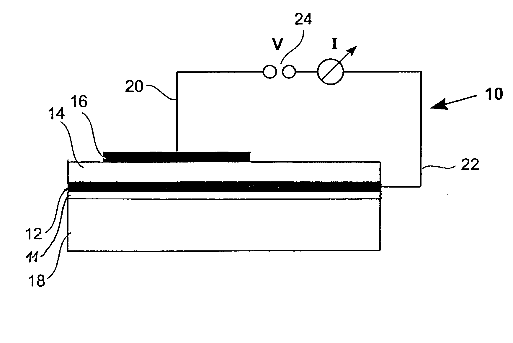
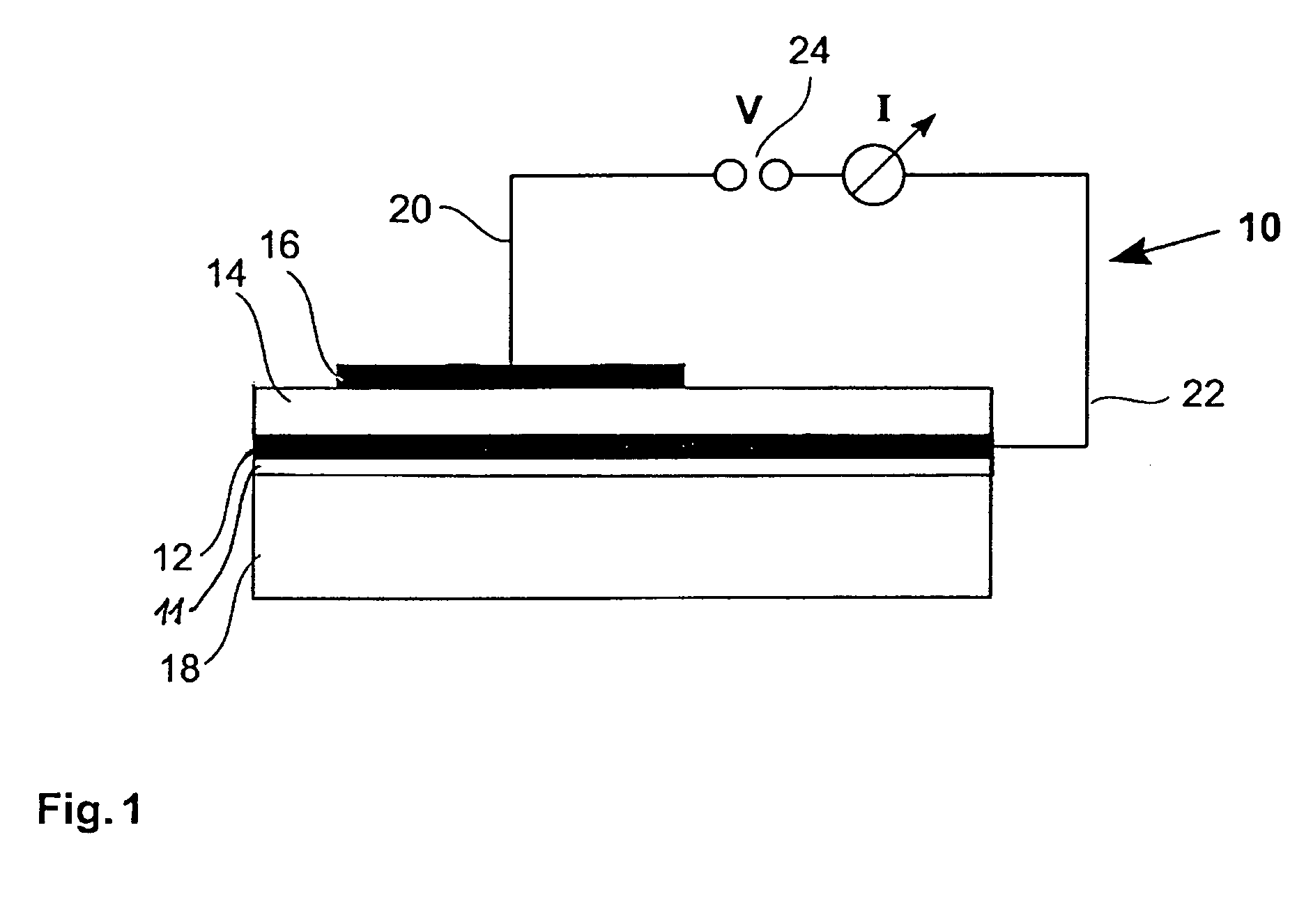
[0019] The present invention provides a process for depositing a switching material that is switchable between at least a first conductivity state and a second conductivity state, each of the states being persistent. An example of a process comprises a step of depositing the switching material by a standard complementary-metal-oxide-semiconductor (CMOS) deposition technique at a temperature lower than 400° C. In other words, the switching material is deposited such as to form an essentially amorphous or poly-crystalline layer. That is, the switching material has an amorphous or poly-crystalline structure resulting from the used deposition temperature.

[0020] The process can be used for manufacturing microelectronic devices comprising a non-volatile resistance switching memory element between two electrodes. The switching material provides the functionality of the non-volatile resistance switching memory element, herein also referred to as switching member or switching layer. The swi...


PUM

PropertyMeasurementUnit
Temperatureaaaaaaaaaa

Abstract

Processes, apparatus and systems for depositing a switching material that is switchable between conductivity states and where the states are persistent. The invention further relates to a microelectronic device or non-volatile resistance switching memory comprising the switching material for storing digital information. A process includes a step of depositing the switching material by a CMOS deposition technique at a temperature lower than 400° C.

Description

TECHNICAL FIELD [0001] The present invention is related to a process for depositing a switching material that is switchable between conductivity states and where the states are persistent. The invention further relates to a microelectronic device or non-volatile resistance switching memory comprising the switching material for storing digital information. BACKGROUND OF THE INVENTION [0002] Non-volatile resistance switching memory, particularly memory based on complex metal oxides, is typically either deposited at high temperature, usually at about 800° C., or requires high temperature post-deposition annealing. This makes it impossible to integrate this type of memory in a back end of the line (BEOL) process with standard complementary-metal-oxide-semiconductor (CMOS) technology. For far BEOL integration the allowed temperatures are even more stringent. [0003] Liu et al., Electrical-pulse-induced reversible resistance change effect in magnetoresistive films, Applied Physics Letters,...

Claims


Application Information

Patent Timeline
IPC IPC(8): C23C16/40G11C11/56H01L21/02H01L21/20H01L21/316H01L21/8238H01L21/8246H01L27/10H01L45/00
CPCG11C13/0007G11C2213/31H01L27/101H01L21/31691H01L45/1233H01L45/147H01L45/1625H01L45/04H01L21/02266H01L21/02197H01L21/02271H01L21/02301H10N70/20H10N70/8836H10N70/026H10N70/826
Inventor ALLENSPACH, ROLFBEDNORZ, JOHANNES G.MEIJER, GERHARD INGMARLAM, CHUNG HONSTUTZ, RICHARDWIDMER, DANIEL
Owner GLOBALFOUNDRIES US INC
Learn More