Optical glass element and manufacturing method thereof
a technology of optical glass elements and manufacturing methods, applied in glass tempering apparatuses, instruments, manufacturing tools, etc., can solve the problems of glass shrinkage difference chips and cracks on the border between lens portions and edges, and achieve the effect of low cos
- Summary
- Abstract
- Description
- Claims
- Application Information
AI Technical Summary
Benefits of technology
Problems solved by technology
Method used
Image
Examples
example 1
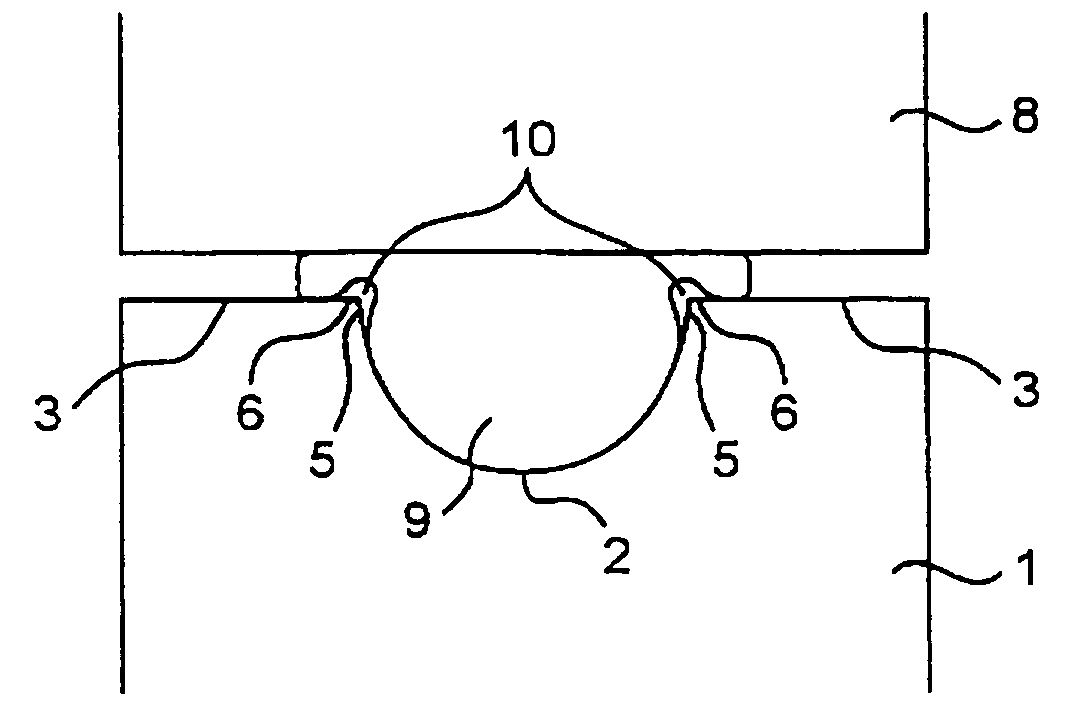
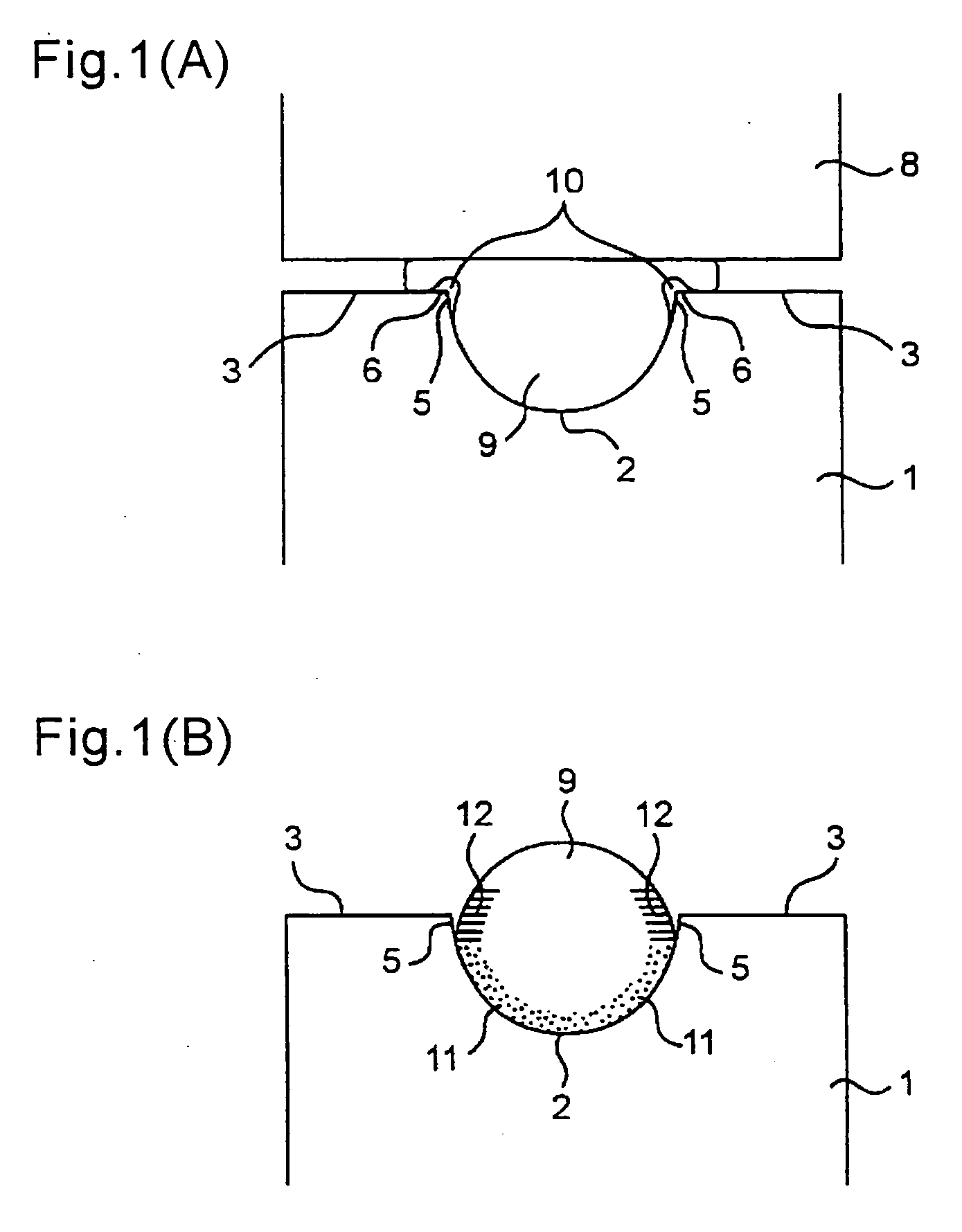
[0064] Optical glass elements were manufactured by using methods as shown in FIGS. 1(A) and 1(B). The lower mold 1 and the upper mold 8 are made of cemented carbide, and each of the molding face and the circumferential face in the lower mold and the upper mold contact face to glass is subjected to a precision polishing process so as to have a surface roughness Ra of 15 nm. With respect to the molding face concave section of the lower mold 1, the opening diameter is 3.2 mm with a depth of 1.5 mm, and the section has a concave non-spherical shape having an approximate radius of curvature of 1.4 mm. The tilt angle of the molding face 2 of the lower mold with respect to the circumferential face 3 is set to 62°. The temperature of the lower mold 1 and the upper mold 8 was set at 450° C.
[0065] More specifically, 70 mg of glass (LaK8), molten at a temperature of 1100° C. in a crucible, not shown, was dropped on the lower-mold molding face through a nozzle heated to 1050° C. so that the di...
example 2
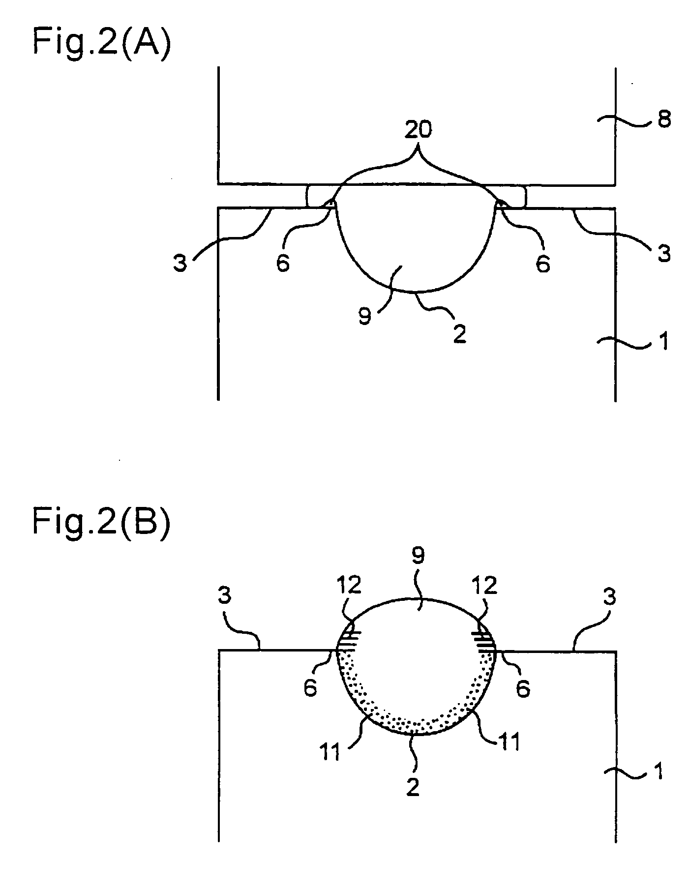
[0070] An optical glass element as shown in FIG. 5(B) was obtained by carrying out the same processes as those of example 1, except that 70 mg of molten glass was dropped from a nozzle so that the diameter of the molten glass droplet was set to 3.2 mm and that this was held in a state as shown in FIG. 2(B) for 6 seconds, and then pressed as shown in FIG. 2(A).
[0071] When the resulting optical glass element was observed under an optical microscope (magnification:×100), it was found that a concave section (groove) was formed in the border between the lens portion and the edge portion with none of cracks and chips being caused therein. The concave section had a free surface, and was located out of an optical effective area. The width w of the concave section was 200 μm with a depth d being set to 100 μm.
[0072] The outer diameter of the lens portion in the element was 4.0 mm, the core thickness thereof was 2.200 mm, the diameter of the optical effective area was 3.0 mm, and the thickn...
example 3
[0073] An optical glass element as shown in FIG. 5(C) was obtained by carrying out the same processes as those of example 1, except that 70 mg of molten glass was dropped from a nozzle so that the diameter of the molten glass droplet was set to 3.0 mm and that this was held in a state as shown in FIG. 3(B) for 5.5 seconds, and then pressed as shown in FIG. 3(A).
[0074] When the resulting optical glass element was observed under an optical microscope (magnification:×100), it was found that a concave section (groove) was formed in the border between the lens portion and the edge portion with none of cracks and chips being caused therein. The concave section had a free surface, and was located out of an optical effective area. The width w of the concave section was 200 μm with a depth d being set to 100 μm.
[0075] The outer diameter of the lens portion in the element was 4.0 mm, the core thickness thereof was 2.200 mm, the diameter of the optical effective area was 3.0 mm, and the thic...
PUM
| Property | Measurement | Unit |
|---|---|---|
| Thickness | aaaaa | aaaaa |
| Thickness | aaaaa | aaaaa |
| Thickness | aaaaa | aaaaa |
Abstract
Description
Claims
Application Information
 - R&D
- Intellectual Property
- Life Sciences
- Materials
- Tech Scout
- Unparalleled Data Quality
- Higher Quality Content
- 60% Fewer Hallucinations
Browse by: Latest US Patents, China's latest patents, Technical Efficacy Thesaurus, Application Domain, Technology Topic, Popular Technical Reports.
© 2025 PatSnap. All rights reserved.Legal|Privacy policy|Modern Slavery Act Transparency Statement|Sitemap|About US| Contact US: help@patsnap.com


