Two-dimensional radiation detector
a two-dimensional radiation and detector technology, applied in the field of semiconductor photon detector arrays, can solve the problems of difficult fabrication of arrays and thus cost, and achieve the effect of good level photoconductive current and high substrate conductivity
- Summary
- Abstract
- Description
- Claims
- Application Information
AI Technical Summary
Benefits of technology
Problems solved by technology
Method used
Image
Examples
Embodiment Construction
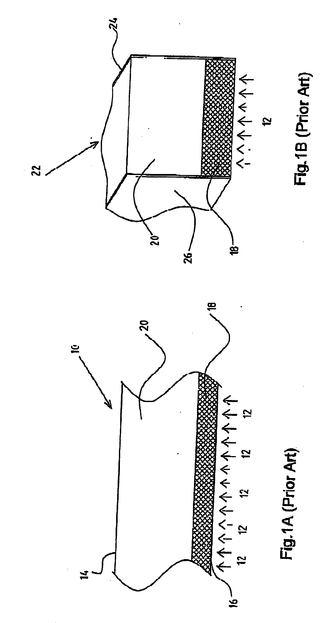
[0032] Reference is now made to FIG. 1A, which schematically illustrates the cross-section of a prior art, parallel-mode, photoconductive detector 10, with the photon flux 12 impinging on the detector in the same direction as the bias field. The bias field is applied between anode 14 and cathode 16 on opposite faces of the detector crystal. The effect of the incident flux of photons is to produce a low resistance layer 18 in the region where the absorption takes place, but in the remainder of the detector depth 20, the resistivity remains at its original high level. As a result, the current through the detector remains limited by the high resistance region, and the resulting sensitivity to the photon illumination is low. This explains a major disadvantage of the parallel mode of operation of such photoconductive detector arrays.
[0033] Reference is now made to FIG. 1B, which schematically illustrates the cross-section of the end view of a prior art, perpendicular-mode, photoconducti...
PUM
 Abstract
Description
Claims
Application Information
 - R&D
- Intellectual Property
- Life Sciences
- Materials
- Tech Scout
- Unparalleled Data Quality
- Higher Quality Content
- 60% Fewer Hallucinations
Browse by: Latest US Patents, China's latest patents, Technical Efficacy Thesaurus, Application Domain, Technology Topic, Popular Technical Reports.
© 2025 PatSnap. All rights reserved.Legal|Privacy policy|Modern Slavery Act Transparency Statement|Sitemap|About US| Contact US: help@patsnap.com


