
Method and system for forming a film of material using plasmon assisted chemical reactions

a technology of chemical reaction and film, applied in the field of processing materials, can solve the problems of high cost of integrated circuit or chip fabrication facilities, difficult devices, and limited process use, and achieve the effect of low power density and high degree of temporal control

Active Publication Date: 2005-10-20
CALIFORNIA INST OF TECH +2
View PDF10 Cites 15 Cited by
  • Summary
  • Abstract
  • Description
  • Claims
  • Application Information

AI Technical Summary

Benefits of technology

[0011] We understand that many materials synthesis methods often require energy in the form of heat. As an example, chemical vapor deposition is a common technique for materials synthesis. Such methods often apply the heat generated by photon-electron interactions in nanometer sized structures as a source of heat for such chemical vapor deposition. In particular, the invention includes use of selected frequencies and / or frequency ranges of electromagnetic radiation in the form of light to control the relative temperature of nanometer sized particles by which material is synthesized. Preferably, the present invention also allows use of simple light sources such as a laser and conventional optics to selectively heat the structures with substantially lower power densities than is otherwise possible with other techniques according to a specific embodiment. It allows for spatial control of material synthesis reactions on the scale of nanometers in certain embodiments. It also allows a high degree of temporal control of the temperature of the synthesis process. These and other features will be described throughout the present specification and more particularly below.
[0027] Many benefits are achieved by way of the present invention over conventional techniques. For example, the present technique provides an easy to use process that relies upon conventional technology. In some embodiments, the method provides higher device yields in dies per wafer. Additionally, the method provides a process that is compatible with conventional process technology without substantial modifications to conventional equipment and processes. Preferably, the invention provides for an improved process integration for design rules of tens of nanometers and less. Additionally, the invention can provide for selective film formation of line widths ranging from about one half of a micron and less or less than one nanometer depending upon the embodiment. Moreover, the present invention includes methods and resulting structures that can be implanted using much tighter controls that conventional processing techniques such as conventional chemical vapor deposition according to preferred embodiments. Still further, the present invention provides a method and resulting structure where plasmon assisted treatment initiates formation of a film of material with control over a resulting film on a pre-form. Such film has a similar or same geometry as the pre-form and electromagnetic radiation used to excite the pre-form is provided using selected temporal control according to a specific embodiment. Depending upon the embodiment, one or more of these benefits may be achieved. These and other benefits will be described in more throughout the present specification and more particularly below.

Problems solved by technology

An integrated circuit or chip fabrication facility can cost hundreds of millions, or even billions, of U.S. dollars.
Making devices smaller is very challenging, as each process used in integrated fabrication has a limit.
Additionally, as devices require faster and faster designs, process limitations exist with certain conventional processes and materials.
The laser spots, however, often require a high power laser source, which is not efficient and costly.
Although CVD and LCVD have had certain success, many limitations still exist.
That is, line widths associated with these processes often cannot be less than a predetermined amount, i.e., diffraction limit of light.
Additionally, film quality often degrades as line widths become smaller.

Method used


Image

  • Method and system for forming a film of material using plasmon assisted chemical reactions
  • Method and system for forming a film of material using plasmon assisted chemical reactions
  • Method and system for forming a film of material using plasmon assisted chemical reactions

Examples


examples

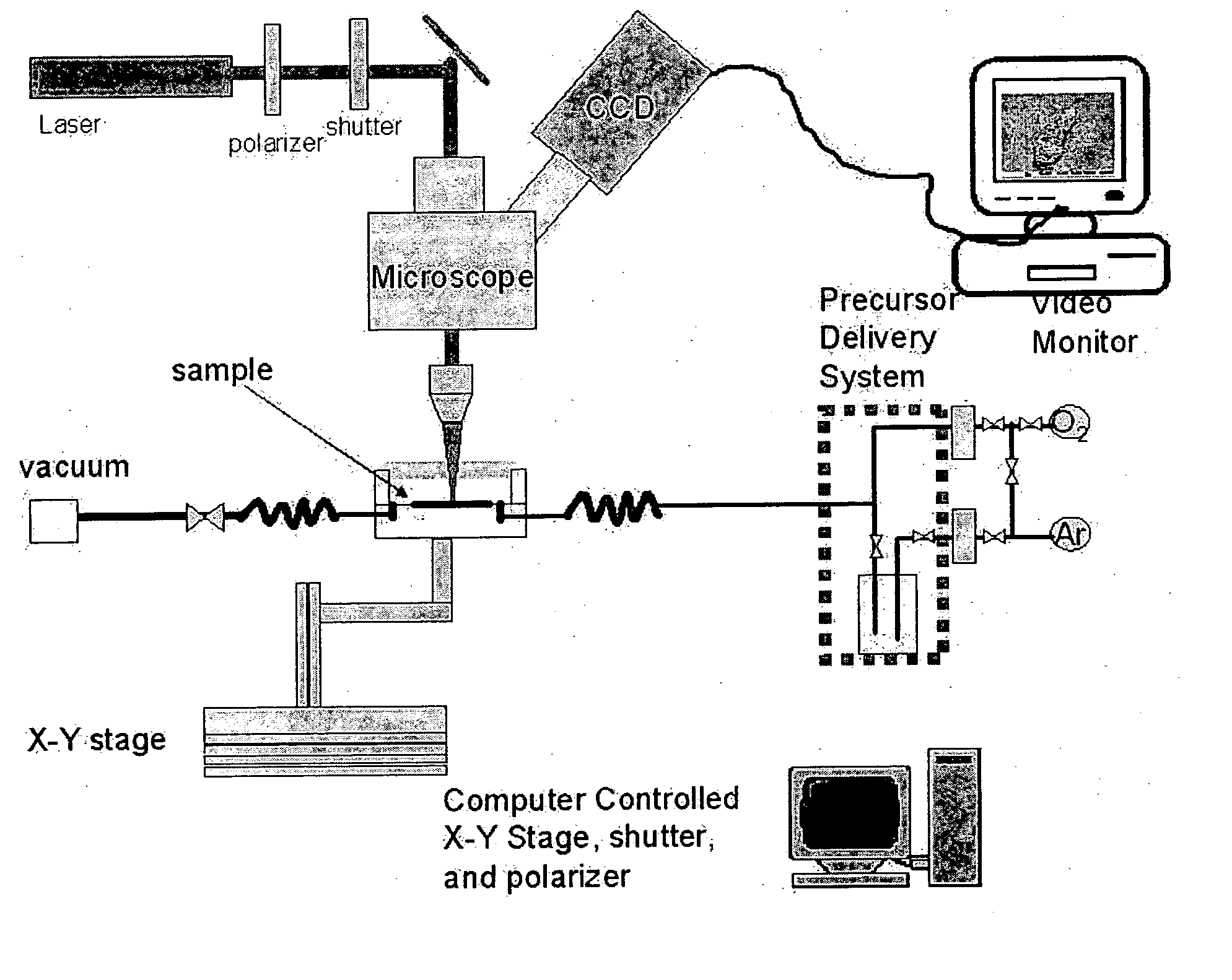
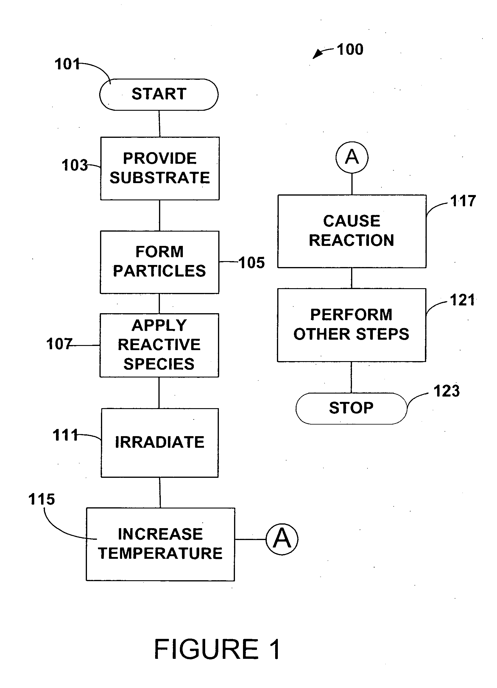
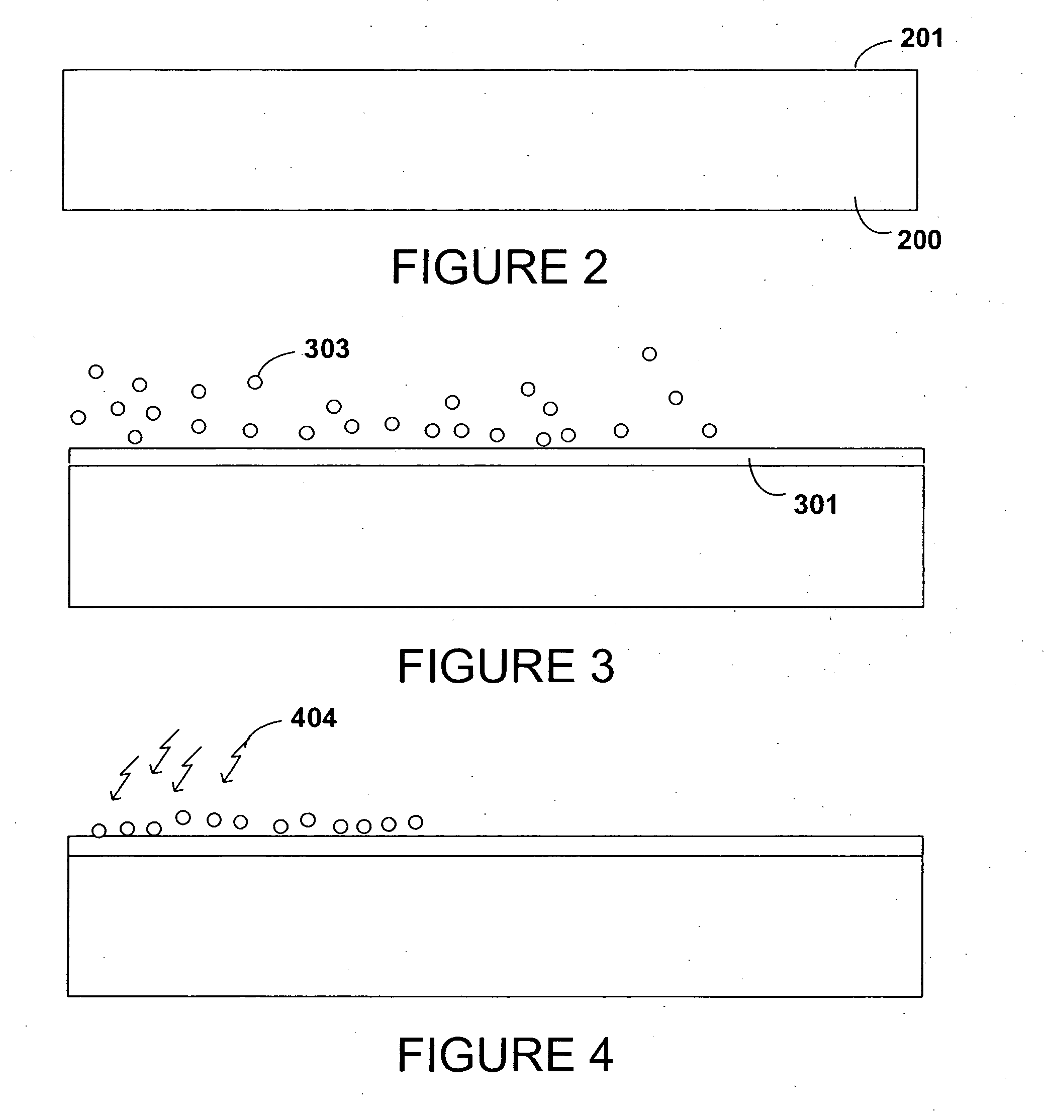
[0081] To prove the principles and operation of the present invention, we have provided examples of the invention in a chemical vapor deposition environment. Such examples are merely illustrative and should not unduly limit the scope of the claims herein. One of ordinary skill in the art would recognize many variations, modifications, and alternatives. As background information, we have provided certain information associated with conventional chemical vapor deposition and its application associated with the present method and systems. One of our goals of present CVD research is to locally control the nanostructure. Ferroelectric materials are highly desirable for non-volatile memory applications. However, there are challenges with fabrication a uniform nano-scale array of ferroelectric material. Conventional CVD provides only random deposition process and is therefore limited.

[0082] In the present example, instead of focusing a laser to locally heat the substrate as in LCVD, local...


PUM

PropertyMeasurementUnit
lengthaaaaaaaaaa
lengthaaaaaaaaaa
diametersaaaaaaaaaa

Abstract

A method for forming a film of material using chemical vapor deposition. The method includes providing a substrate comprising a pattern of at least one metallic nanostructure, which is made of a selected material. The method includes determining a plasmon resonant frequency of the selected material of the nanostructure and exciting a portion of the selected material using an electromagnetic source having a predetermined frequency at the plasmon resonant frequency to cause an increase in thermal energy of the selected material. The method includes applying one or more chemical precursors overlying the substrate including the selected material excited at the plasmon resonant frequency and causing selective deposition of a film overlying at least the portion of the selected material.

Description

CROSS-REFERENCE TO RELATED APPLICATIONS [0001] This present application claims priority to U.S. Provisional Ser. No. 60 / 529,869 filed Dec. 15, 2003, commonly assigned and hereby incorporated by reference for all purposes.STATEMENT AS TO RIGHTS TO INVENTIONS MADE UNDER FEDERALLY SPONSORED RESEARCH OR DEVELOPMENT [0002] N / A BACKGROUND OF THE INVENTION [0003] The present invention is directed to processing materials and in particular micro or nanostructures and their applications. More particularly, the present invention provides methods and resulting structures for forming nano and micro structures using a deposition technique for a wide variety of applications. As merely an example, such deposition techniques can be applied to formation of one or more films in the manufacture of electronic devices, such as integrated circuits. But it would be recognized that the invention has a much broader range of applicability. The present invention may be used for etching, enhancing chemical reac...

Claims


Application Information

Patent Timeline
Patent Type & Authority Applications(United States)
IPC IPC(8): B81C1/00C23C16/00C23C16/02C23C16/04C23C16/40C23C16/48
CPCB81C1/00111C23C16/0281C23C16/483C23C16/405C23C16/047B82Y30/00C23C16/34H01L21/02365
Inventor BOYD, DAVID A.BRONGERSMA, MARKGREENGARD, LESLIE
Owner CALIFORNIA INST OF TECH
Learn More