
Organic electroluminescence device

Inactive Publication Date: 2005-10-13
IDEMITSU KOSAN CO LTD
View PDF6 Cites 5 Cited by
  • Summary
  • Abstract
  • Description
  • Claims
  • Application Information

AI Technical Summary

Benefits of technology

[0015] (1) From the standpoint of enhancing the property of the light emitting host molecules to catch holes when the light emitting guest molecules are mixed, it is preferable that the host material has an energy gap of 2.8 eV or greater. The reason is that, when the energy gap is great, the ionization energy of the host material is increased and the host material can work more effectively as the hole trap even when the same light emitting guest molecules are used. In particular, this case is preferable for obtaining emission of blue light.
[0016] (2) From the standpoint of improving the balance between the amounts of electrons and holes in the construction having the layer of the host material and the layer of a metal complex, it is preferable that the layer of the host material has the hole transporting property. The hole transporting property is defined as the charge transporting property when the mobility of holes is greater than the mobility of electrons and can be measured in accordance with a conventional method such as the method of time of flight.
[0062] By laminating the layer comprising a specific N,N,N′,N′-tetra(biphenyl)diaminoarylene derivative to the light emitting layer, the balance between the amounts of electrons and holes is improved. Therefore, injection of holes into the electron injecting layer is suppressed and deterioration of the electron injecting layer is prevented. As the result, the organic EL device can exhibit a higher efficiency and have a longer life.
[0063] In the present invention, further improvements in the performance can be achieved by laminating the layer comprising a specific N,N,N′,N′-tetra(biphenyl)diaminoarylene derivative and further by using a layer of a metal complex having an energy gap of 2.8 eV or greater as the electron injecting layer.
[0070] Examples of the reducing dopant include at least one alkali metal selected from the group consisting of Na (the work function: 2.36 eV), K (the work function: 2.28 eV), Rb (the work function: 2.16 eV) and Cs (the work function: 1.95 eV) and at least one alkaline earth metal selected from the group consisting of Ca (the work function: 2.9 eV), Sr (the work function: 2.0 to 2.5 eV) and Ba (the work function: 2.52 eV). Among these reducing dopants, reducing dopants having a work function of 2.9 eV or smaller are preferable. More preferable reducing dopants are at least one alkali metal selected from the group consisting of K, Rb and Cs. Still more preferable reducing dopants are Rb and Cs and the most preferable reducing dopant is Cs. These alkali metals have high reducing ability and the luminance of emitted light and the life of the organic EL device are improved by adding these alkali metals in a relatively small amount into the region of electron injection. As the reducing dopant having a work function of 2.9 eV or smaller, combinations of two or more alkali metals are preferable and combinations including Cs such as combinations of Cs and Na, Cs and K, Cs and Rb, and Cs, Na and K are more preferable. When Cs is include in the combination, the reducing ability can be efficiently exhibited and the luminance of emitted light and the life of the organic EL device can be improved by adding the combination into the region of electron injection.
[0071] In the present invention, an electron injecting layer constituted with an insulating material or a semiconductor may be disposed between the cathode and the layer of an organic thin film. By disposing the electron injecting layer, leak of electric current can be effectively prevented and the electron injecting property can be improved. It is preferable that at least one metal compound selected from the group consisting of alkali metal chalcogenides, alkaline earth metal chalcogenides, alkali metal halides and alkaline earth metal halides is used as the insulating material. It is preferable that the electron injecting layer is constituted with the alkali metal chalcogenide or the like since the electron injecting property can be further improved. Preferable examples of the alkali metal chalcogenide include Li2O, LiO, Na2S, Na2Se and NaO. Preferable examples of the alkaline earth chalcogenide include CaO, BaO, SrO, BeO, BaS and CaSe. Preferable examples of the alkali metal halide include LiF, NaF, KF, LiCl, KCl and NaCl. Preferable examples of the alkaline earth metal halide include fluorides such as CaF2, BaF2, SrF2, MgF2 and BeF2 and halides other than the fluorides.

Problems solved by technology

As the result of extensive studies by the present inventors to overcome the above problems, it was found that, in a device having a conventional laminate structure having a layer of a host material and a layer of Alq and, in particular, in a device having a laminate structure having a layer of a host material using a phenylanthracene derivative, which is preferable as the host material, and a layer of Alq, (1) injection of electrons from the cathode into the layer of a phenylanthracene derivative is not easy and (2) holes are injected into the layer of Alq and deterioration in the electron injecting layer takes place due to the injection of holes.

Method used


Image

  • Organic electroluminescence device
  • Organic electroluminescence device
  • Organic electroluminescence device

Examples


synthesis example 1

[0078] Into a flask, 1.0 g of trimethoxygallium and 40 ml of anhydrous ethanol were placed and stirred. To the resultant solution, 0.84 g of 4-hydroxybiphenyl was added and the obtained mixture was stirred at 80° C. for 7 hours. Major portions of the solid substance separated as precipitates were dissolved into a hot ethanol and the resultant solution was filtered. The obtained filtrate was concentrated and the resultant concentrate was dried in vacuo to obtain 1.5 g of a yellowish white powder. The yellowish white powder was analyzed in accordance with the mass analysis and found to be gallium chelate compound (28) shown above. The energy gap was measured from absorption end of the light absorption spectrum and found to be 2.95 eV.

synthesis example 2

[0079] The same procedures as those conducted in Synthesis Example 1 were conducted except that 0.59 g of 4-cyanophenol was used in place of 0.84 g of 4-hydroxybiphenyl and 1.4 g of a yellowish white powder was obtained. The yellowish white powder was analyzed in accordance with the mass analysis and found to be gallium chelate compound (17) shown above. The energy gap was measured from absorption end of the light absorption spectrum and found to be 2.96 eV.

synthesis example 3

[0080] The same procedures as those conducted in Synthesis Example 1 were conducted except that 0.47 g of phenol was used in place of 0.84 g of 4-hydroxybiphenyl and 1.3 g of a yellowish white powder was obtained. The yellowish white powder was analyzed in accordance with the mass analysis and found to be gallium chelate compound (27) shown above. The energy gap was measured from absorption end of the light absorption spectrum and found to be 2.93 eV.

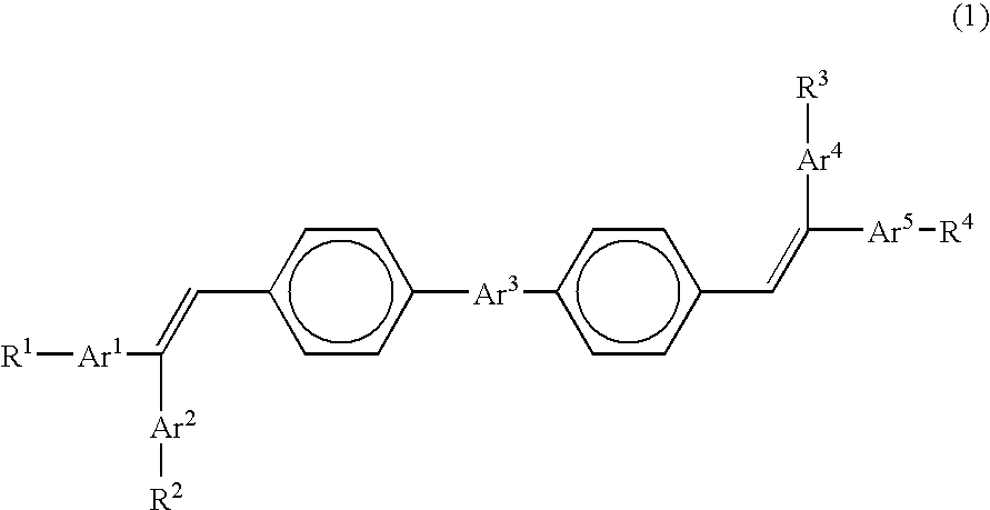
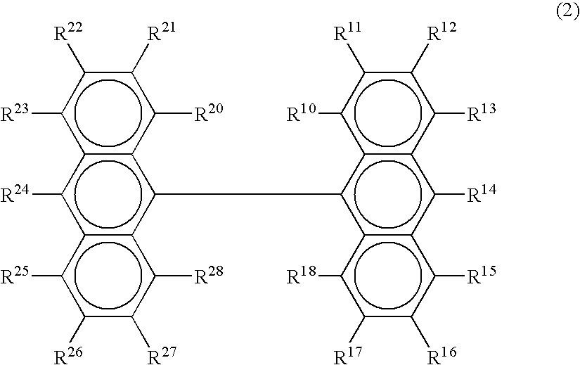
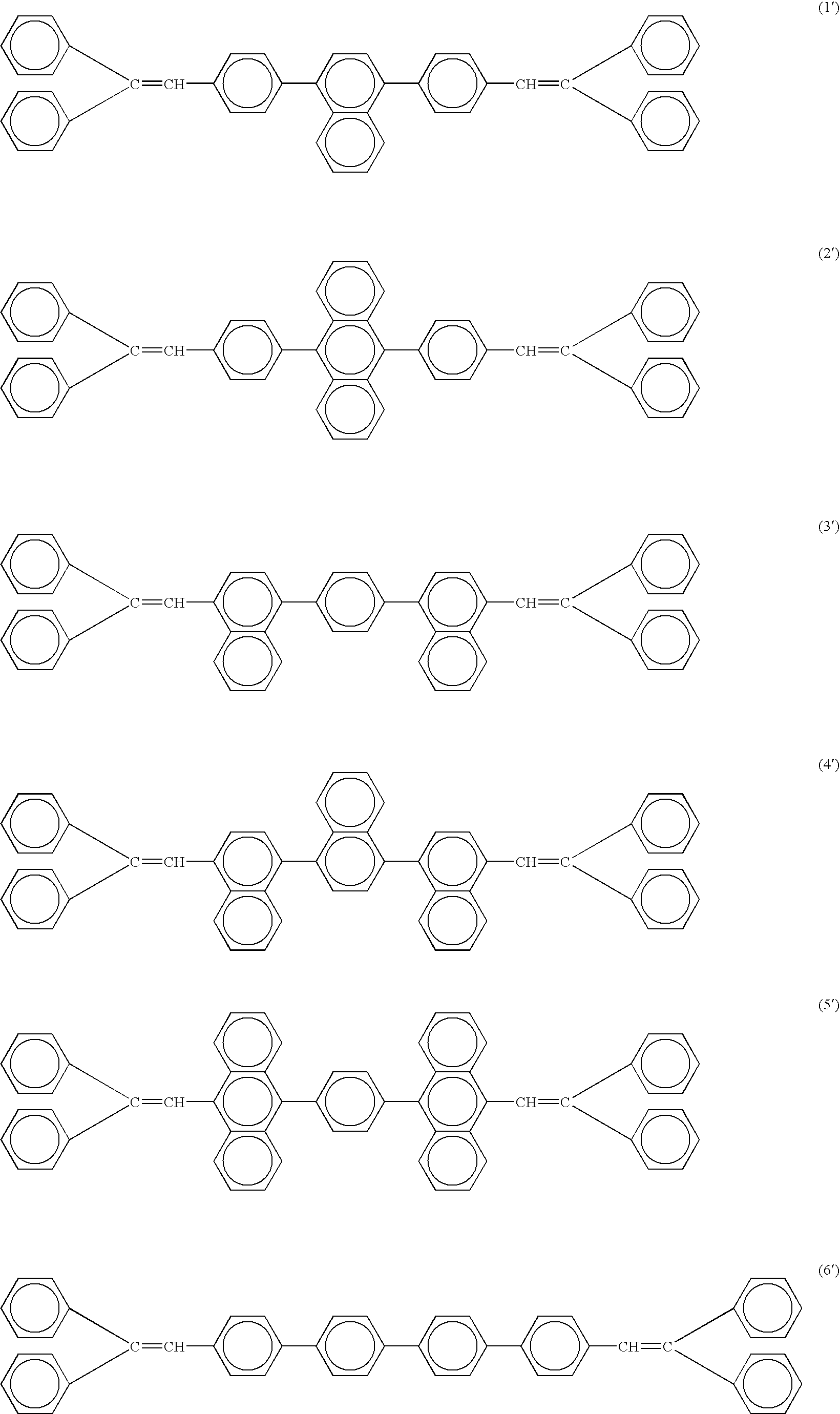
[0081] The chemical structures of the compounds used in Examples and Comparative Examples are shown in the following. The ionization energy and the electron affinity of these compounds are shown in Table 1.

TABLE 1D1D2D3D4D5C1C2C3E1E2E3CompoundIonization energy (eV)Electron affinity (eV)(E1)5.702.80(E2)5.722.73(E3)5.802.79(D1)5.352.45(D2)5.412.53(D3)5.392.51(D4)5.372.56(D5)5.232.65(C1)5.622.89(C2)5.753.25(C3)5.522.78

[0082] The ionization energy (Ip) was measured by using an atmospheric photoelectronic spectrophotometer AC1 manufacture...


PUM

PropertyMeasurementUnit
Energyaaaaaaaaaa
Energy gapaaaaaaaaaa
Energyaaaaaaaaaa

Abstract

An organic electroluminescence device comprises a cathode, an anode and a layer of an organic thin film comprising one or a plurality of layers and disposed between the cathode and the anode, wherein at least one of the layers in the layer of an organic thin film comprises a laminate of a layer comprising a metal complex having an energy gap of 2.8 eV or greater and a layer of a host material. The organic electroluminescence device exhibits a higher efficiency of light emission and has a longer life than conventional devices while the emitted light has a high luminance.

Description

TECHNICAL FIELD [0001] The present invention relates to an organic electroluminescence device and, more particularly, to an organic electroluminescence device emitting light of a high luminance at a high efficiency and having a long life. BACKGROUND ART [0002] An organic electroluminescence device (hereinafter, referred to as an organic EL device) is a spontaneous light emitting device which utilizes the principle that a fluorescent substance emits light by recombination of holes injected from an anode and electrons injected from a cathode when an electric field is applied. [0003] Since an organic EL device of the laminate type driven under a low electric voltage was reported by C. W. Tang of Eastman Kodak Company (C. W. Tang and S. A. Vanslyke, Applied Physics Letters, Volume 51, Pages 913, 1987), many studies have been conducted on organic EL devices using organic materials as the constituting materials. Tang et al used tris(8-hydroxyquinolinol)aluminum as the light emitting layer...

Claims


Application Information

Patent Timeline
IPC IPC(8): C09K11/06H01L51/00H01L51/30H01L51/50H01L51/52
CPCB32B9/00Y10T428/24942C09K2211/1003C09K2211/1007C09K2211/1011C09K2211/1014C09K2211/1029C09K2211/188H01L51/0054H01L51/0058H01L51/0059H01L51/006H01L51/0079H01L51/0081H01L51/0082H01L51/5012H01L51/5048H01L51/5092H01L51/5221H01L2251/308Y10S428/917C09K11/06H10K85/622H10K85/626H10K85/633H10K85/321H10K85/631H10K85/326H10K85/324H10K50/14H10K50/171H10K50/82H10K50/11H10K2102/103H05B33/14
Inventor HOSOKAWA, CHISHIOFUNAHASHI, MASAKAZUSAKAI, TOSHIOARAKANE, TAKASHIYAMAMOTO, HIROSHI
Owner IDEMITSU KOSAN CO LTD
Learn More