Binary frequency-shift keying demodulator
- Summary
- Abstract
- Description
- Claims
- Application Information
AI Technical Summary
Benefits of technology
Problems solved by technology
Method used
Image
Examples
Embodiment Construction
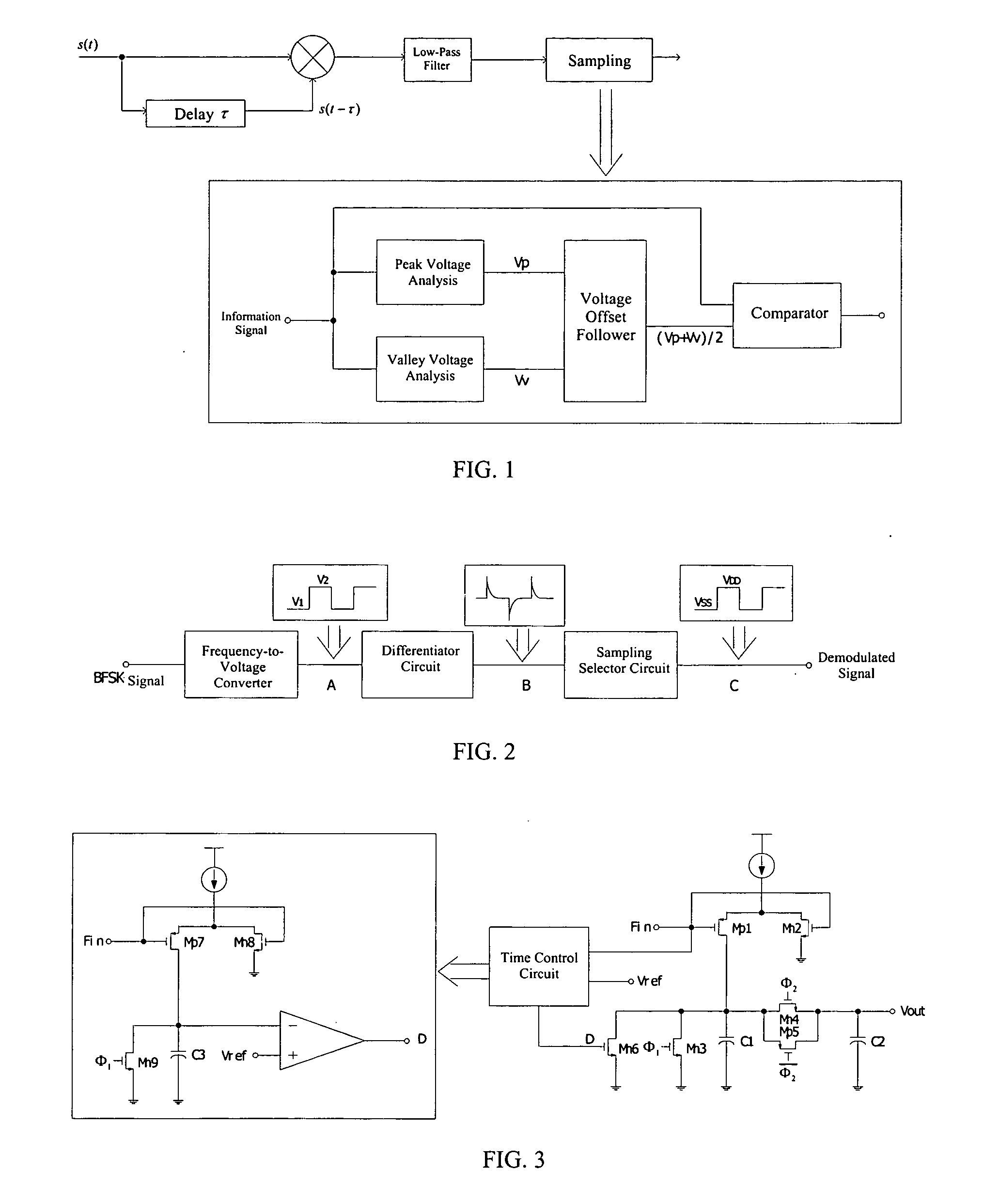
[0010] As is seen in FIG. 2, the present invention provides a Binary Frequency-Shift Keying Demodulator comprising a frequency-to-voltage converter, a differentiator circuit, and a sampling selector circuit. A BFSK signal is input to a frequency-voltage converter. A square wave output signal is produced by the frequency-voltage converter as shown on step A. Frequencies fc+Δf and fc−Δf (fc is carrier wave frequency) match voltage V1 and V2, respectively (V12). Since the voltage difference at step A may be too narrow to active a logic circuit to transform this demodulated signal at step A into digital, the signal at step A is differentiated by a differentiator circuit, having an output signal at step B. The signal at step B is filtered by a sampling selector circuit to produce a voltage signal output C. The signal at step C is the demodulated signal.
[0011] The output voltage wave from the frequency-to-voltage converter has various spikes from the discreteness caused by charge injecti...
PUM
 Abstract
Description
Claims
Application Information
 - R&D
- Intellectual Property
- Life Sciences
- Materials
- Tech Scout
- Unparalleled Data Quality
- Higher Quality Content
- 60% Fewer Hallucinations
Browse by: Latest US Patents, China's latest patents, Technical Efficacy Thesaurus, Application Domain, Technology Topic, Popular Technical Reports.
© 2025 PatSnap. All rights reserved.Legal|Privacy policy|Modern Slavery Act Transparency Statement|Sitemap|About US| Contact US: help@patsnap.com


