Evaluation chip
a technology of eva chips and chips, applied in the field of eva chips, can solve problems such as the inability to use eva chips
- Summary
- Abstract
- Description
- Claims
- Application Information
AI Technical Summary
Benefits of technology
Problems solved by technology
Method used
Image

Examples
working example 1
Configuration
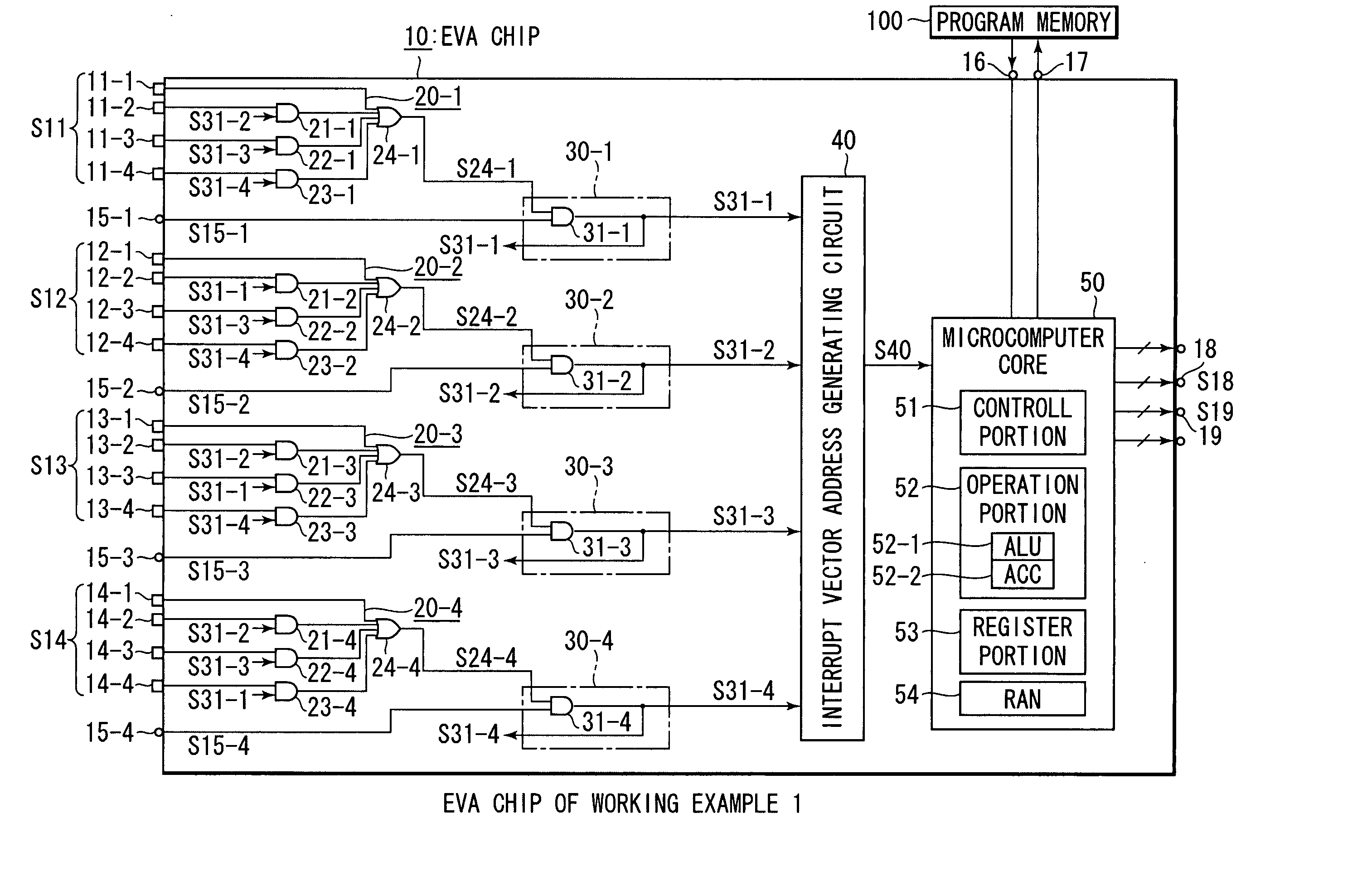
[0021]FIG. 1 a view of a schematic diagram showing an EVA chip 10 according to a first working example, Working Example 1, of the present invention.
[0022] The EVA chip 10 evaluates a program that is stored in an external program memory 100. The EVA chip 10 includes four sets of control signal input terminals 11-1 to 11-4, 12-1 to 12-4, 13-1 to 13-4, and 14-1 to 14-4, four interrupt request signal input terminals 15-1 to 15-4, an instruction input terminal 16, an address output terminal 17, a plurality of data output terminals 18, and a plurality of control signal output terminals 19. A plurality (for example, four) of four-bit control signals S11, S12, S13, and S14 used for interrupt priority order modifying control for the program is respectively input into the four sets of control signal input terminals 11-1 to 11-4, 12-1 to 12-4, 13-1 to 13-4, and 141 to 14-4. Four interrupt request signals are input into the four interrupt request signal input terminals 15-1 to 1...
working example 2
Configuration
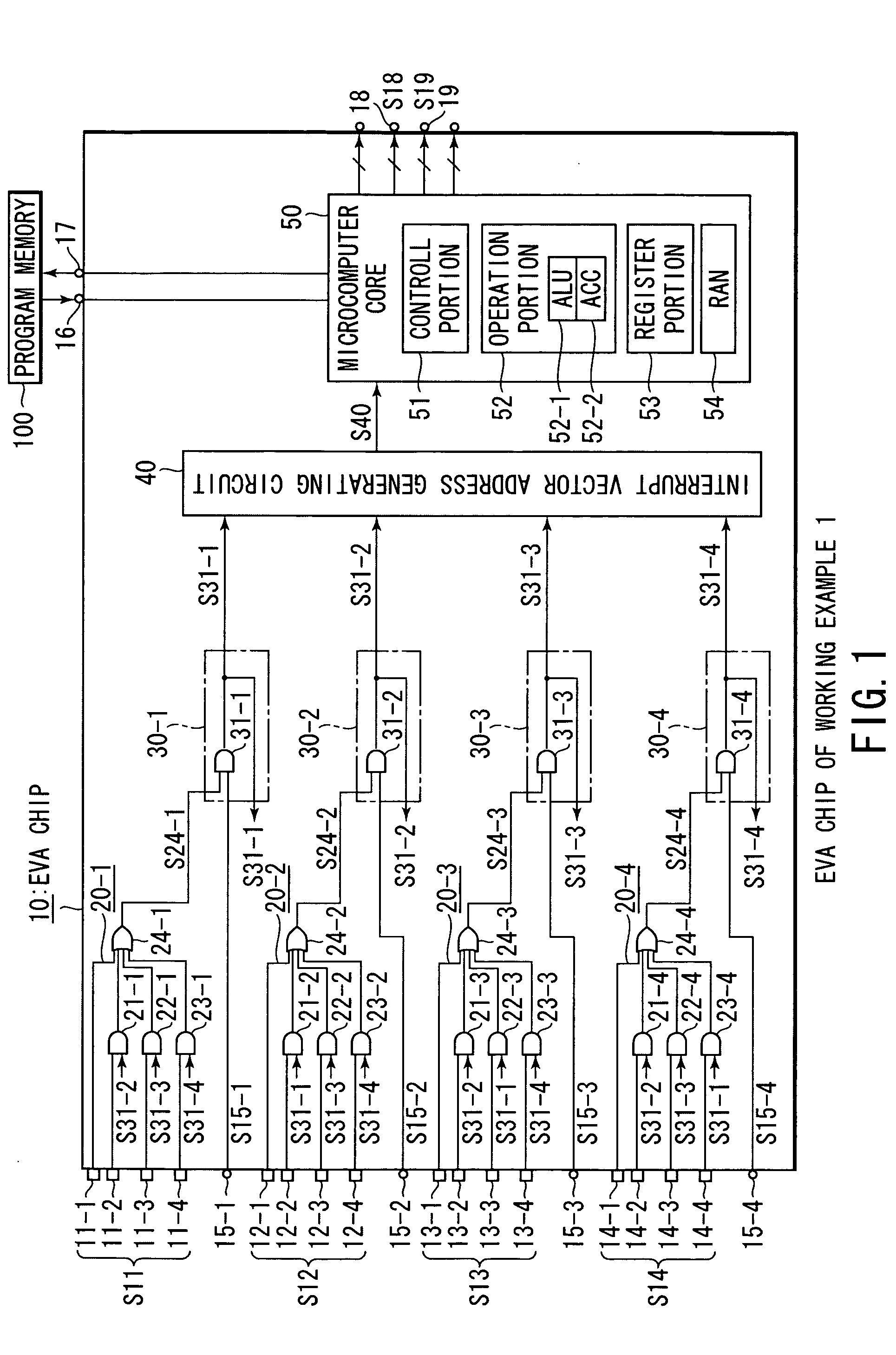
[0042]FIG. 2 is a schematic diagram showing an EVA chip 10A according to a second working example, Working Example 2, of the present invention. Like symbols are used for structural elements that are the same as or similar to those in FIG. 1 of Working Example 1.
[0043] In the EVA chip 10 of Working Example 1, the control signal input terminals 11-1 to 11-4, 12-1 to 12-4, 13-1 to 13-4, and 14-1 to 14-4 are provided to switch the interrupt priority order of the interrupt modules 30-1 to 30-4. In the EVA chip 10A of Working Example 2, on the other hand, four data input terminals 61 to 64 and four priority order control registers 71 to 74 that are respectively connected to these terminals are provided instead of the control signal input terminals 11-1 to 11-4, 12-1 to 12-4, 13-1 to 13-4, and 14-1 to 14-4.
[0044] Data regarding the interrupt priority order are input to the data input terminals 61 to 64 from a CPU that controls the EVA chip 10A. The priority order control r...
working example 3
Configuration
[0057]FIG. 3 is a schematic diagram of an EVA chip 10B according to a third working example, Working Example 3, of the present invention. Like symbols are used for structural elements that are the same as in Working Example 1 in FIG. 1 and Working Example 2 FIG. 2.
[0058] In the EVA chip 10A of Working Example 2, data input terminals 61 to 64 and priority order control registers 71 to 74 are provided to switch the interrupt priority order of the interrupt modules 30-1 to 30-4. In the EVA chip 10B of Working Example 3, on the other hand, three input terminals 81 to 83 and a 12-bit interrupt priority order control shift registers 90 that is connected to these terminals are provided instead of the data input terminals 61 to 64 and the priority order control registers 71 to 74.
[0059] At the input terminal 81, serial 12-bit priority order data S81 are input from outside; at the input terminal 82, a synchronization clock S82 is input from outside; and at the input terminal...
PUM
 Abstract
Description
Claims
Application Information
 - R&D
- Intellectual Property
- Life Sciences
- Materials
- Tech Scout
- Unparalleled Data Quality
- Higher Quality Content
- 60% Fewer Hallucinations
Browse by: Latest US Patents, China's latest patents, Technical Efficacy Thesaurus, Application Domain, Technology Topic, Popular Technical Reports.
© 2025 PatSnap. All rights reserved.Legal|Privacy policy|Modern Slavery Act Transparency Statement|Sitemap|About US| Contact US: help@patsnap.com