Method for attaching shields on substrates
- Summary
- Abstract
- Description
- Claims
- Application Information
AI Technical Summary
Benefits of technology
Problems solved by technology
Method used
Image
Examples
Example
DETAILED DESCRIPTION OF THE DRAWINGS
[0023] While the specification concludes with claims defining the features of several embodiments of the invention that are regarded as novel, it is believed that the invention will be better understood from a consideration of the following description in conjunction with the drawing figures, in which like reference numerals are carried forward.
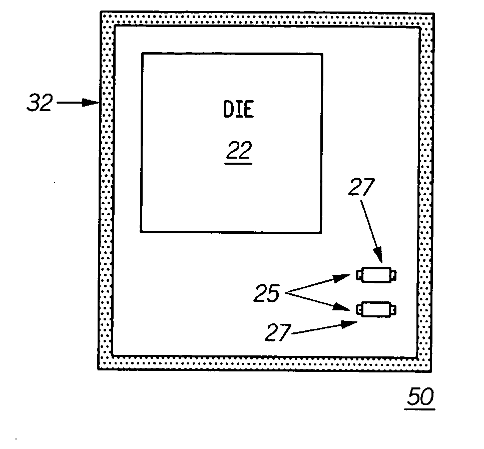
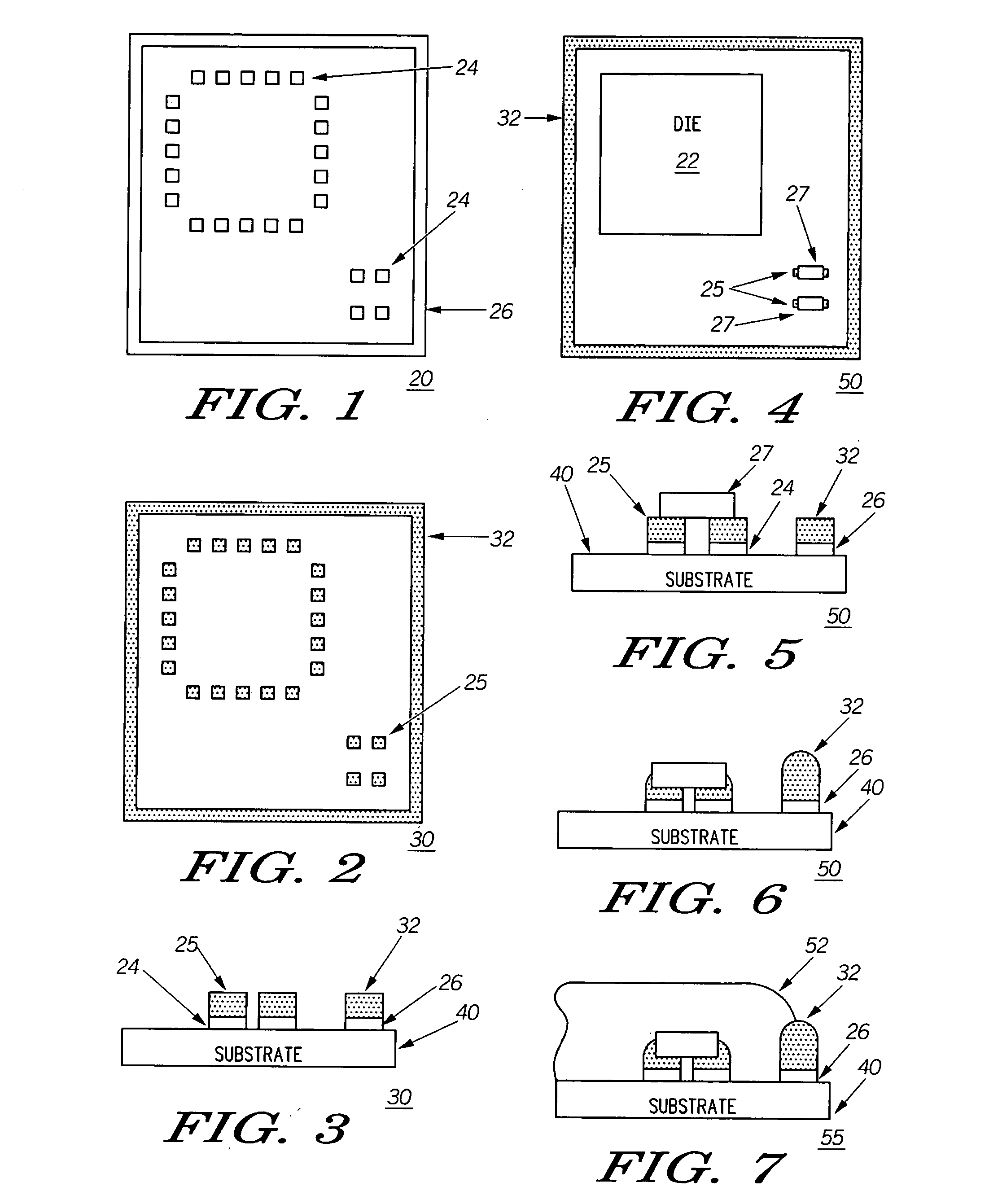
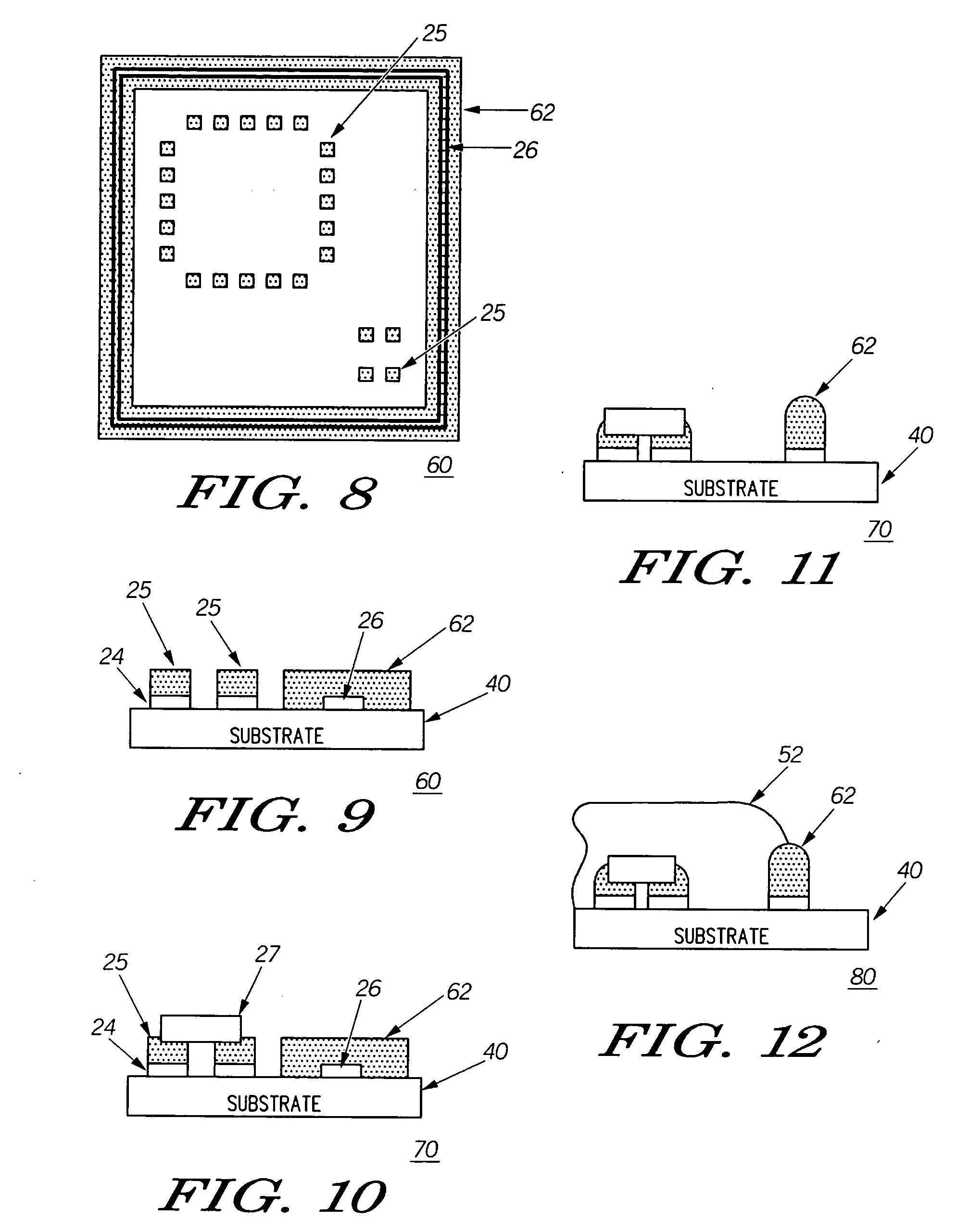
[0024] Referring now to FIGS. 1-12, a substrate assembly such as in the form of a processed printed circuit board 20 can include a predetermined area on a substrate 40 defined by a metallized trace pattern 26 serving as a shield track. The trace pattern can be created during the printed circuit board (PCB) manufacturing process. Thus, a preprinted PCB would include a pattern ready for solder application during a normal solder screen printing operation, for example. In this manner, a separate step (as done in attaching existing shields using conductive epoxy) is eliminated. A pre-printed PCB 30 or 60 (as s...
PUM
 Abstract
Description
Claims
Application Information
 - R&D
- Intellectual Property
- Life Sciences
- Materials
- Tech Scout
- Unparalleled Data Quality
- Higher Quality Content
- 60% Fewer Hallucinations
Browse by: Latest US Patents, China's latest patents, Technical Efficacy Thesaurus, Application Domain, Technology Topic, Popular Technical Reports.
© 2025 PatSnap. All rights reserved.Legal|Privacy policy|Modern Slavery Act Transparency Statement|Sitemap|About US| Contact US: help@patsnap.com


