Semiconductor light emitting device capable of suppressing silver migration of reflection film made of silver
a technology of silver reflection film and semiconductor, applied in the direction of semiconductor device, basic electric element, electrical apparatus, etc., can solve the problem of insufficient migration suppression effect, and achieve the effect of suppressing the ionization of metal constituting the reflection film and suppressing the generation of migration
- Summary
- Abstract
- Description
- Claims
- Application Information
AI Technical Summary
Benefits of technology
Problems solved by technology
Method used
Image
Examples
first embodiment
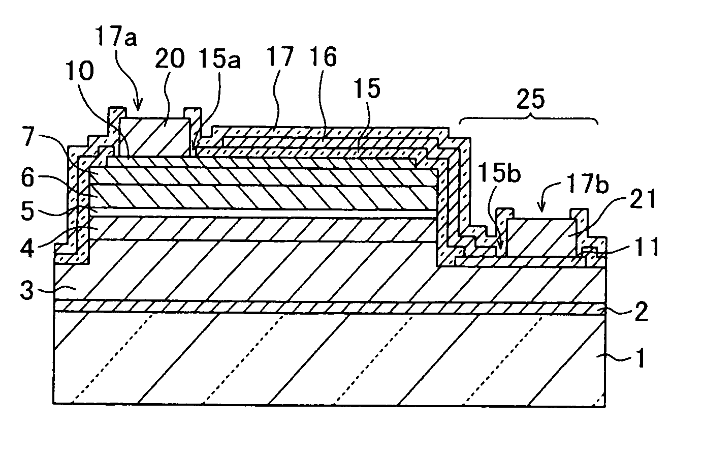
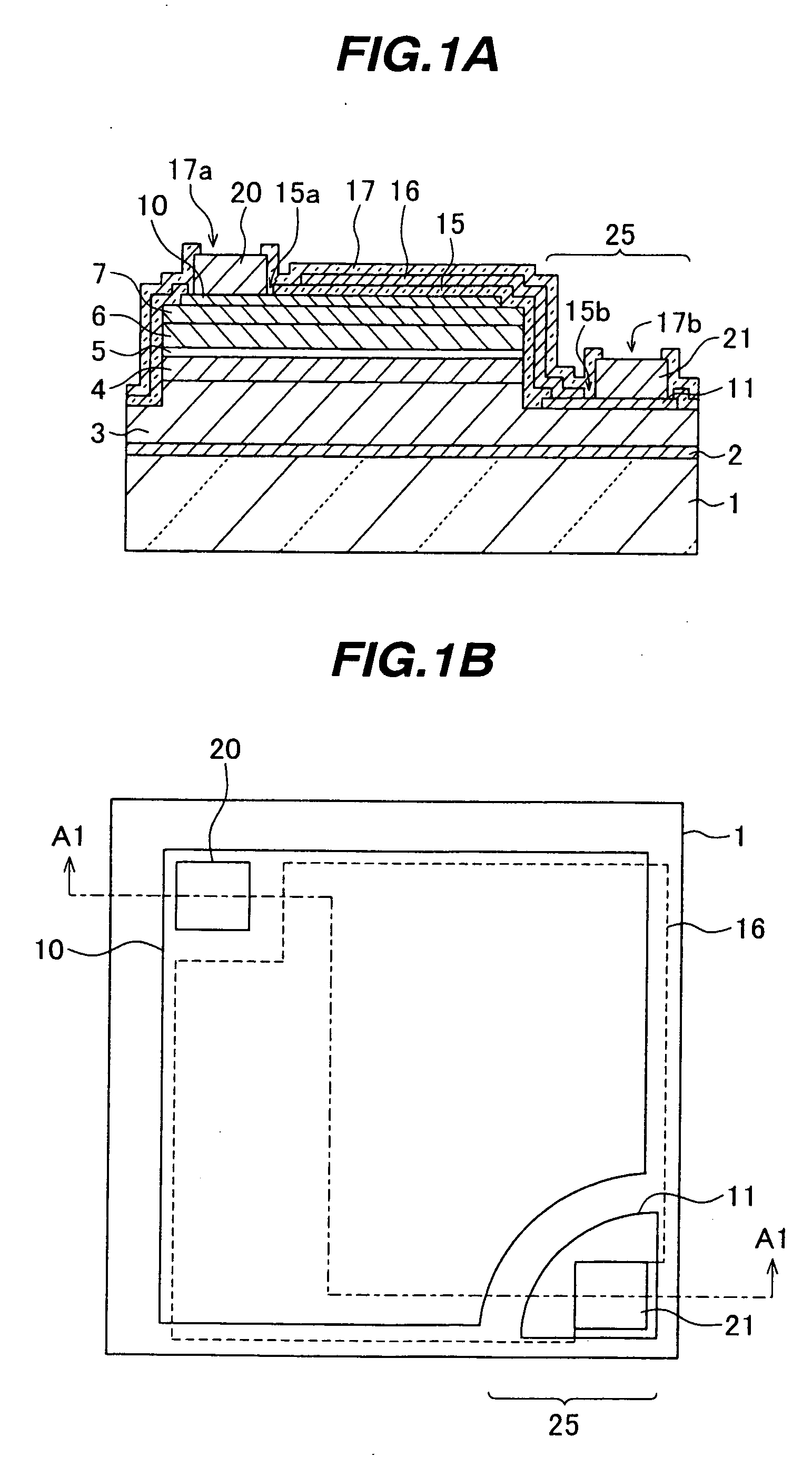
[0041]FIG. 1A is a cross sectional view of a semiconductor light emitting device and FIG. 1B is a plan view of the device shown in FIG. 1A. A cross sectional view taken along one-dot chain line A1-A1 shown in FIG. 1B corresponds to FIG. 1A. On an underlying substrate 1 made of sapphire, an initial nucleus forming layer 2, an n-type contact layer 3, an n-type clad layer 4, a luminous layer 5, a p-type clad layer 6, a p-type contact layer 7 are stacked in this order. These layers are made of nitride compound semiconductor such as InxAlyGazN (x+y+z=1).
[0042] In a first area 25 of a partial substrate in-plane, the layers from the p-type contact layer 7 to a surface layer of the n-type contact layer 3 are etched to partially expose the n-type contact layer 3.
[0043] A p-side ohmic electrode 10 is formed on the p-type contact layer 7. The p-side ohmic electrode 10 is made of platinum (Pt) and has a thickness of about 5 nm. An n-side ohmic electrode 11 is formed on the surface of the n-ty...
second embodiment
[0083] Next, with reference to FIGS. 10 and 11, a semiconductor light emitting device of the second embodiment will be described.
[0084]FIG. 10 is a plan view of a semiconductor light emitting device of the second embodiment. In the first embodiment shown in FIG. 1B, the reflection film 16 is made of a plain film and superposes most area of the p-side ohmic electrode 10. In the second embodiment, in place of the reflection film 16, a reflection pattern 16a of a grid shape is disposed. The other fundamental structure is similar to that of the semiconductor light emitting device of the first embodiment. In the example shown in FIG. 10, although a p-side pad electrode 20 and an n-side pad electrode 21 are disposed slightly inside of the central area of a pair of opposing sides of a rectangle, they may be disposed near at the vertexes of the rectangle as in the case of the first embodiment shown in FIG. 1B.
[0085] In the semiconductor light emitting device of the second embodiment, light...
third embodiment
[0091] Next, with reference to FIGS. 12A and 12B and FIG. 13, a semiconductor light emitting device of the third embodiment will be described.
[0092]FIG. 12A is a cross sectional view of the semiconductor light emitting device of the third embodiment, and FIG. 12B is a plan view thereof. A cross sectional view taken along one-dot chain line A12-A12 shown in FIG. 12B corresponds to FIG. 12A. Description will be made on different points from the semiconductor light emitting device of the first embodiment.
[0093] In the first embodiment, the n-side pad electrode 21 is disposed on the n-side ohmic electrode 11, whereas in the second embodiment, an n-side pad electrode 21 is disposed over a p-side ohmic electrode 10 and contacts a reflection film 16. A p-side pad electrode 20 and the n-side pad electrode 21 are exposed on the bottoms of openings 17a and 17b formed through a protective film 17.
[0094] As shown in FIG. 12B, the n-side ohmic electrode 11 is disposed along one side of a suppo...
PUM
 Abstract
Description
Claims
Application Information
 - R&D
- Intellectual Property
- Life Sciences
- Materials
- Tech Scout
- Unparalleled Data Quality
- Higher Quality Content
- 60% Fewer Hallucinations
Browse by: Latest US Patents, China's latest patents, Technical Efficacy Thesaurus, Application Domain, Technology Topic, Popular Technical Reports.
© 2025 PatSnap. All rights reserved.Legal|Privacy policy|Modern Slavery Act Transparency Statement|Sitemap|About US| Contact US: help@patsnap.com


