Memory control device, data cache control device, central processing device, storage device control method, data cache control method, and cache control method

a control device and data cache technology, applied in the field of memory control devices, can solve the problems of ensuring tso preservation between the processors alone, affecting the processing efficiency of the storage device,

Inactive Publication Date: 2005-09-22
FUJITSU LTD
View PDF6 Cites 34 Cited by
  • Summary
  • Abstract
  • Description
  • Claims
  • Application Information

AI Technical Summary

Benefits of technology

[0022] A memory control device according to still another aspect of the present invention is shared by a plurality of threads that are concurrently executed and that processes memory access requests issued by the threads. The memory control device includes an access invalidating unit that, when the instruction processor switches threads, invalidates from among store instructions and fetch instructions issued by the thread being inactivated, all the store instructions and fetch instructions that are not committed; and an interlocking unit that, when the inactivated thread is reactivated, detects the fetch instructions that are influenced by the execution of the committed store instructions, and exerts control in such a way that the detected fetch instructions are executed after the store instructions.
[0023] A memory device control method according to still another aspect of the present invention is a method for processing memory access requests issued from concurrently executed threads. The memory device control method includes determining, when storing data belonging to an address specified in the memory access request, whether a first thread is the same as a second thread, wherein the first thread is a thread that has registered the data and the second thread is a thread that has issued the memory access request; and activating a coherence ensuring mechanism that ensures coherence in a sequence of execution of reading and writing of the data by a plurality of instruction processors, wherein the data is shared between the instruction processors.
[0024] A data cache control method according to still another aspect of the present invention is a method for processing memory access requests issued from concurrently executed threads. The data cache control method includes determining, when storing a cache line that includes data belonging to an address specified in the memory access request, whether a first thread is the same as a second thread, wherein the first thread is a thread that has registered the cache line and the second thread is a thread that has issued the memory access request; and activating a coherence ensuring mechanism that ensures coherence in a sequence of execution of reading and writing of the data by a plurality of instruction processors, wherein the data is shared between the instruction processors.
[0025] A cache control method according to still another aspect of the present invention is used by a central processing device that includes a plurality of sets of instruction processors that concurrently execute a plurality of threads and primary data cache devices, and a secondary cache device that is shared by the primary data cache devices belonging to different sets. The cache control method includes each of the primary data cache device making to the secondary cache device a cache line retrieval request when the cache line belonging to a physical address that matches with the physical address in the memory access request from the instruction processor; the secondary cache device performing throwing-out, when the cache line retrieval request is registered in the primary data cache device by another thread, the secondary cache device makes to the primary cache device a request to invalidate or throw out the cache line; and the primary data cache device activating, by invalidating or throwing out the cache line based on the request from the secondary cache device, the coherence ensuring mechanism that ensures coherence of a sequence of execution of reading of and writing to the cache line by a plurality of instruction processors, the cache line being shared by the primary data cache device belonging to other sets.
[0026] A data cache control method according to still another aspect of the present invention is a method for processing memory access requests issued from concurrently executed threads. The memory device control method includes invalidating, when the instruction processor switches threads, from among store instructions and fetch instruction issued by the thread being inactivated, all the store instructions and fetch instructions that are not committed; and detecting, when the inactivated thread is reactivated, the fetch instructions that are influenced by the execution of the committed store instructions, and executing control in such a way that the detected fetch instructions are executed after the store instructions.

Problems solved by technology

However, the out-of-order process can produce a Total Store Order (TSO) violation if there is a write involved, in which case, going back and reading the stalled data would mean reading an outdated data.
However, ensuring TSO preservation between the processors alone is inadequate in a computer system implementing a multi-thread method.

Method used


Image

  • Memory control device, data cache control device, central processing device, storage device control method, data cache control method, and cache control method
  • Memory control device, data cache control device, central processing device, storage device control method, data cache control method, and cache control method
  • Memory control device, data cache control device, central processing device, storage device control method, data cache control method, and cache control method

Examples


second embodiment

[0069] In the first embodiment, the RIM flag of the fetch port was set with the aid of synonym control of the secondary cache unit or a cache line throw out request by the primary data cache unit. However, the secondary cache unit may not have a mechanism for carrying out synonym control, and the primary data cache unit may not have a mechanism for carrying out cache line throw out request.

[0070] Therefore, in a second embodiment of the present invention, TSO is ensured by monitoring the throwing out / invalidation process of replacement blocks produced during the replacement of the cache lines or by monitoring access requests for accessing the cache memory or the main storage device. Since primarily the operation of the cache controller in the second embodiment is different from the first embodiment, the operation of the cache controller is explained here.

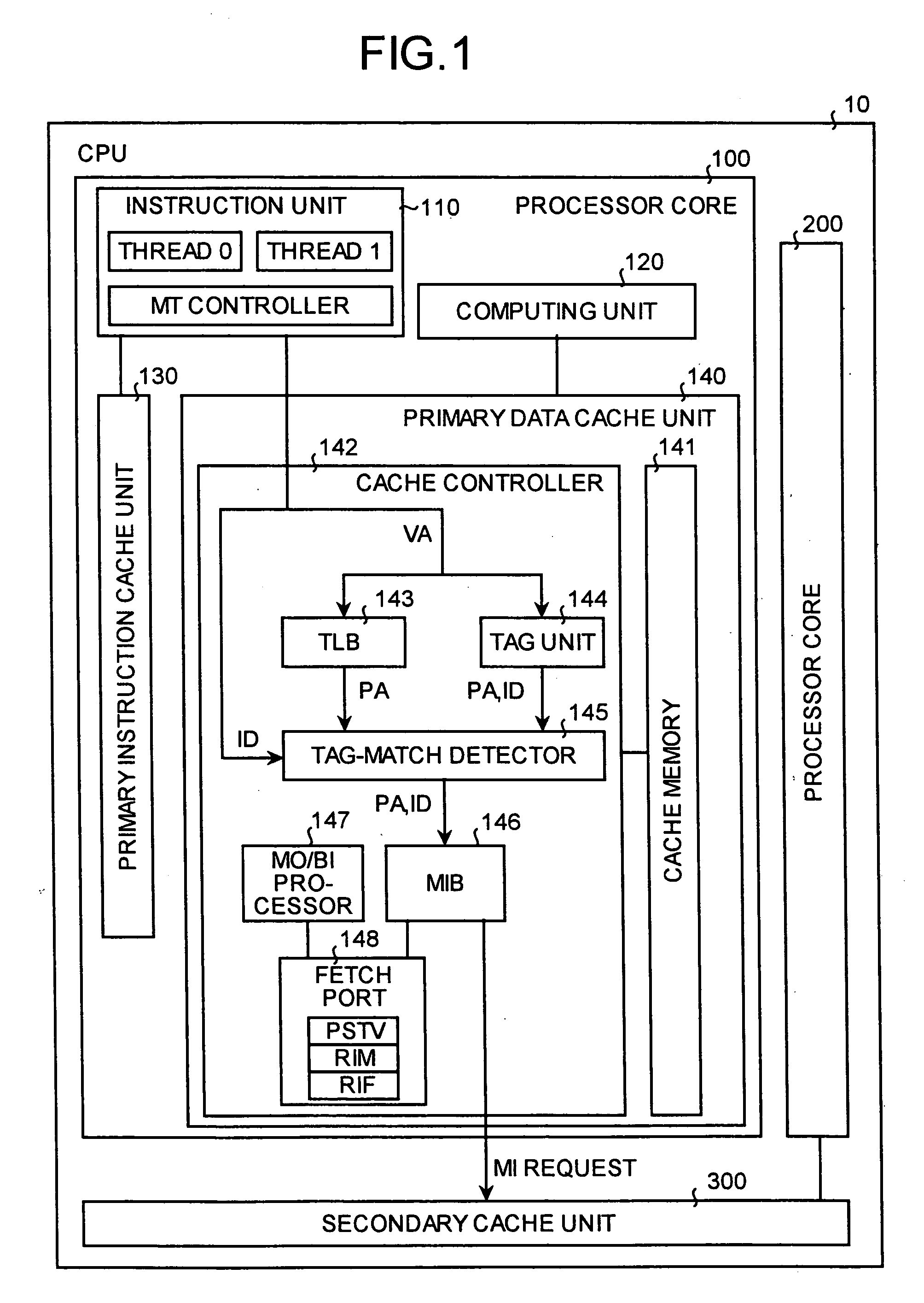
[0071] The structure of a CPU according to the second embodiment is explained next. FIG. 5 is a functional block diagram of the ...


PUM


Abstract

A central processing device includes a plurality of sets of instruction processors that concurrently execute a plurality of threads and primary data cache devices. A secondary cache device is shared by the primary data cache device belonging to different sets. The central processing device also includes a primary data cache unit and a secondary cache unit. The primary data cache unit makes an MI request to the secondary cache unit when a cache line with a matching physical address but a different thread identifier is registered in a cache memory, performs an MO / BI based on the request from the secondary cache unit, and sets a RIM flag of a fetch port. The secondary cache unit makes a request to the primary cache unit to perform the MO / BI when the cache line for which MI request is received is stored in the primary data cache unit by a different thread.

Description

BACKGROUND OF THE INVENTION [0001] 1) Field of the Invention [0002] The present invention relates to a memory control device, a data cache control device, a central processing device, a storage device control method, a data cache control method, and a cache control method that process a request to access memory, issued concurrently from a plurality of threads [0003] 2) Description of the Related Art [0004] The high-performance processors, which have become commonplace of late, use what is known as an out-of-order process for processing instructions while preserving instruction level parallelism. The out-of-order process involves stalling the process of reading data of an instruction that has resulted in a cache miss, reading the data of a successive instruction, and then going back to reading the data of the stalled instruction. [0005] However, the out-of-order process can produce a Total Store Order (TSO) violation if there is a write involved, in which case, going back and reading...

Claims


Application Information

Patent Timeline
Patent Type & Authority Applications(United States)
IPC IPC(8): G06F12/00G06F12/08
CPCG06F9/3824G06F12/0815G06F9/3851G06F9/3834
Inventor YAMAZAKI, IWAO
Owner FUJITSU LTD
Why Eureka
Try Eureka