
Redundancy structure and method for high-speed serial link

a high-speed serial link and redundancy technology, applied in the field of data communication, can solve the problems of increasing the likelihood that a receiver or a transmitter will fail at some time, unsuitable for use in high-speed serdes cores operating at signal switching speeds above 500 mhz

Inactive Publication Date: 2005-08-18
IBM CORP
View PDF32 Cites 16 Cited by
  • Summary
  • Abstract
  • Description
  • Claims
  • Application Information

AI Technical Summary

Benefits of technology

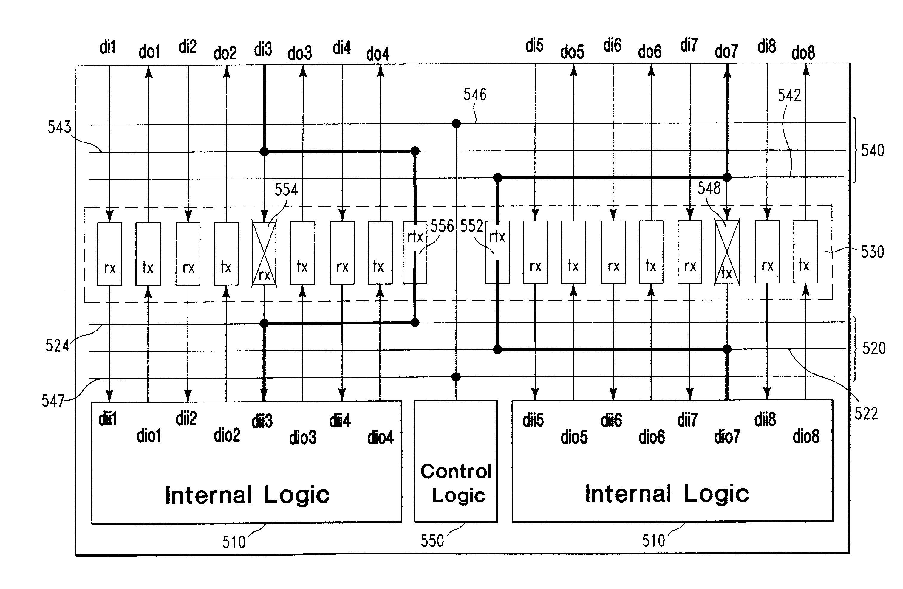
[0011] An integrated circuit is provided having a plurality of data transmitters operable at signal switching frequencies above about 500 MHz, including a plurality of default data transmitters for transmitting data from a plurality of data sources and at least one redundancy data transmitter. A plurality of connection elements are provided having a first, low impedance connecting state at frequencies above about 500 MHz and having

Problems solved by technology

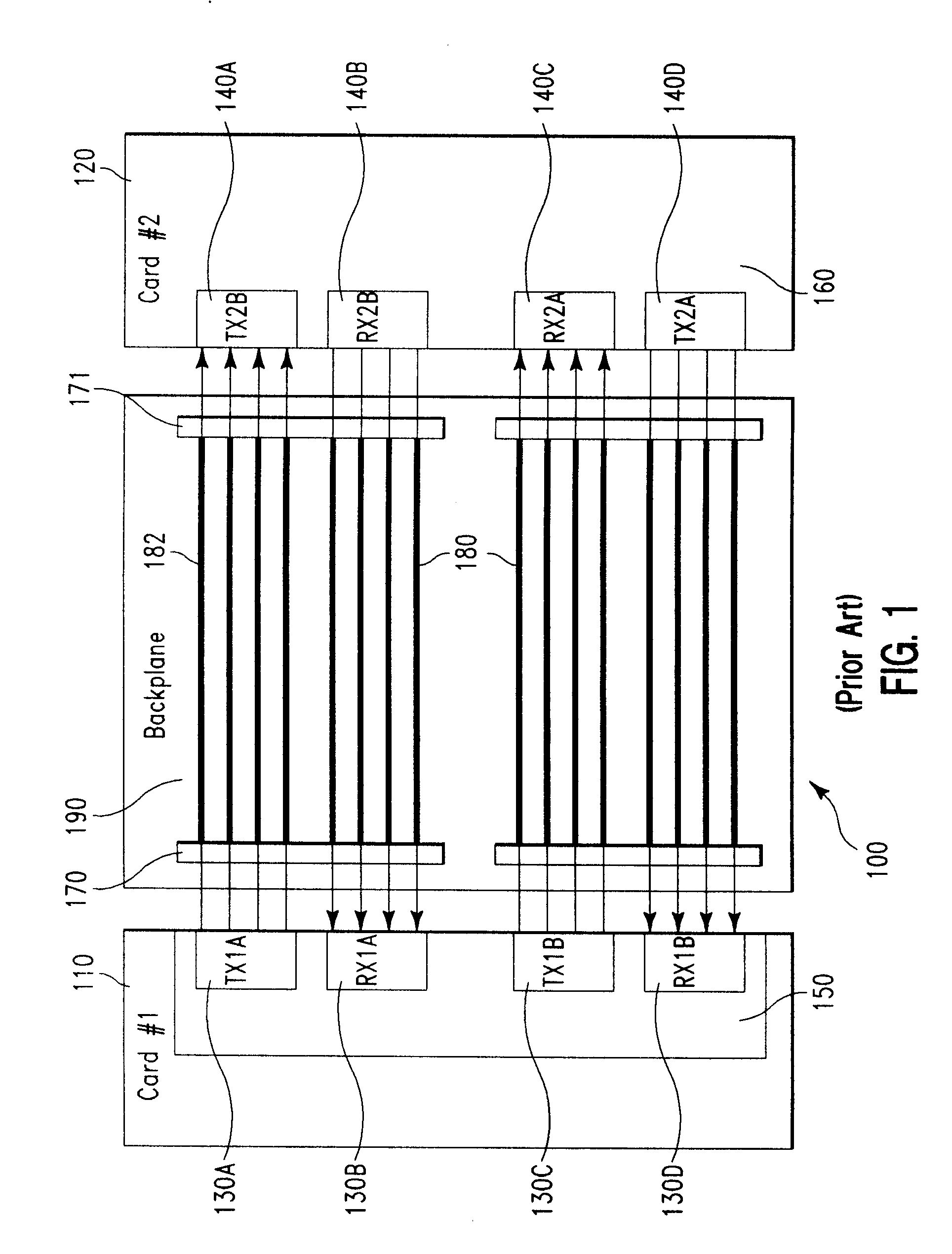
Given the operational performance required from each transmitter and receiver, and the number of receivers and transmitters provided in each chip having a SerDes core, it is likely that one or more receivers and transmitters on a chip will fail at some time, either during post-production testing or later when installed for use.
As the number of receivers and transmitters per chip is increased, the likelihood that a receiver or a transmitter will fail increases further.
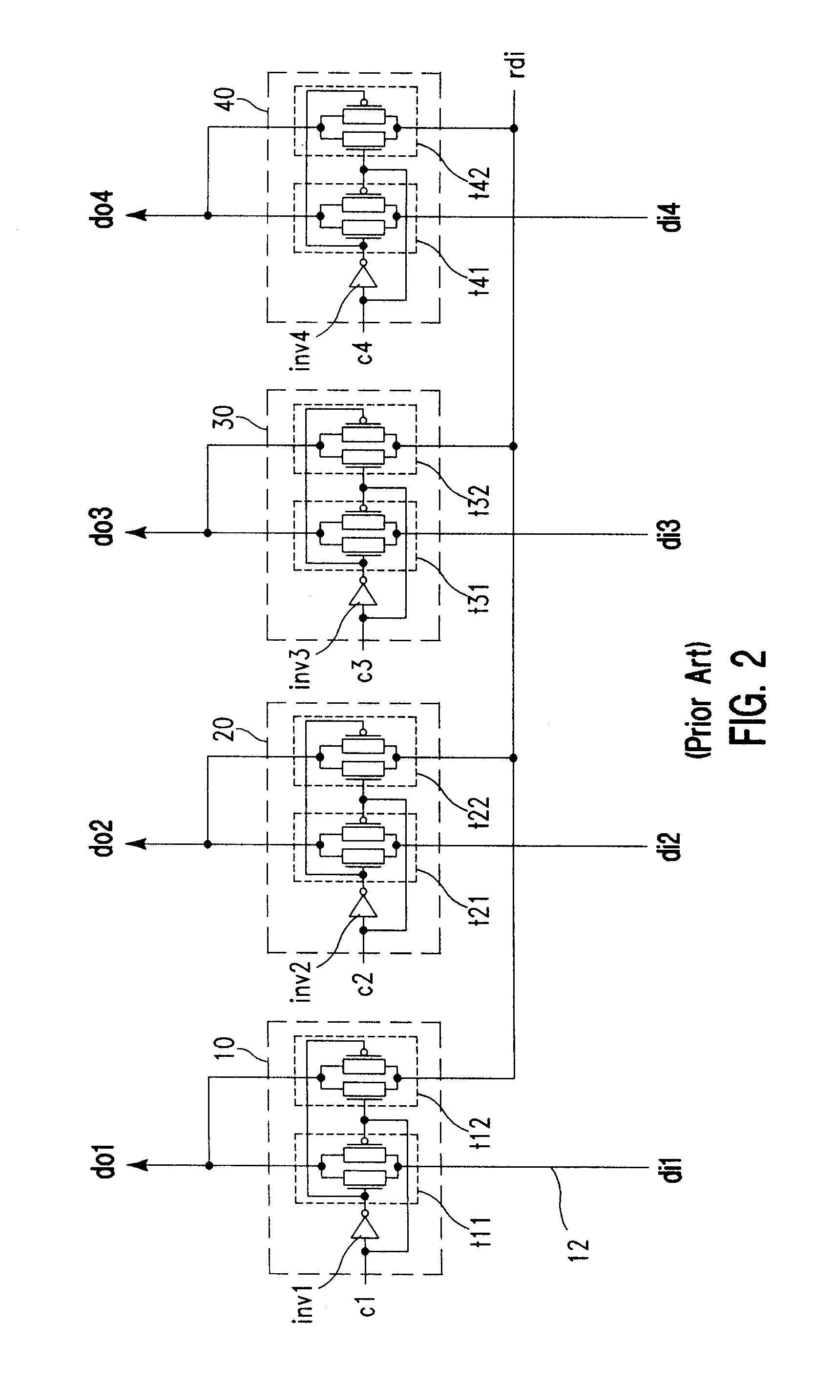
While the prior art arrangement shown in FIG. 2 performs acceptably within a memory array, twoTwo problems of the prior art arrangement of FIG. 2 make it unsuitable for use in high-speed SerDes cores operating at signal switching speeds above about 500 MHz.
Second, the redundancy signal path from redundancy signal line rdi to output signal line suffers from high parasitic junction capacitance.
Such parasitic junction capacitance reduces the transmission bandwidth of signals on the redundancy signal input line rdi even more so than the jitter noise caused by the transmission gates of the default signal path.
Both of these problems make redundancy replacement arrangements using MOSFET transmission gates unsuitable for signal switching speeds above about 500 MHz.

Method used


Image

  • Redundancy structure and method for high-speed serial link
  • Redundancy structure and method for high-speed serial link
  • Redundancy structure and method for high-speed serial link

Examples


Embodiment Construction

[0019]FIG. 3 is a schematic diagram of a redundancy replacement arrangement according to a first preferred embodiment the invention. In such embodiment, a plurality of input signal lines di1 through di4 are connected to outputs of individual transmitters of one of the transmitter blocks 130A or 130C (FIG. 1). In the embodiment shown in FIG. 3, a plurality of connection elements 210, 220, 230 and 240 are provided, each having a fuse and an antifuse, for connecting the input signal lines di1 through di4 to corresponding ones of the output signal lines do1 through do4. Thus, by default, transmitters of a transmitter block 130A or 130C, which are connected to the input signal lines di1 through di4, are normally connected by a set of corresponding fuses f1, f2, f3, and f4 to the output signal lines do1 through do4. A fuse initially presents low impedance. Upon application of sufficient electrical conditions, the fuse is blown, which changes the fuse to a highly resistive, high impedance ...


PUM


Abstract

An integrated circuit is provided having a plurality of data transmitters, including a plurality of default data transmitters for transmitting data from a plurality of data sources and at least one redundancy data transmitter. A plurality of connection elements are provided having a first, low impedance connecting state and having a second, high impedance, disconnecting state. The connection elements are operable to disconnect a failing data transmitter from a corresponding output signal line and to connect the redundancy data transmitter to that output signal line in place of the failing data transmitter. In one preferred form, the connection elements include a fuse and an antifuse. In another form, the connection elements include micro-electromechanical (MEM) switches. The connecting elements preferably present the low impedance connecting state at frequencies which include signal switching frequencies above about 500 MHz.

Description

BACKGROUND OF INVENTION [0001] The present invention relates to data communications and more specifically to a structure and method for redundancy replacement in high-speed data communications circuitry. [0002] Different types of systems are available today for providing high-speed data communications. Some systems require all communications to be transmitted using the same communication protocol layer stack. Other systems require communications to be transmitted at a particular transmission rate. The Unilink family of serializer-deserializer (SerDes) integrated circuits (“ICs” or “chips”)cores offered by the assignee of the present invention, provides flexible choice over the communication protocol layer stack and the transmission rate. [0003] Such SerDes cores chips have multiple adapters cores including data transmitters and receivers for integration into application specific integrated circuits (“ASICs” or “chips”). Chips containing SerDes cores typically include one or more add...

Claims


Application Information

Patent Timeline
IPC IPC(8): H04L1/22H04L25/02H04L25/08H04L27/04
CPCH04L1/22H04L25/08H04L25/029
Inventor HSU, LOUIS L.RADENS, CARLWANG, LI-KONG
Owner IBM CORP
Learn More