Field effect transistor and method for manufacturing the same

a field effect transistor and transistor technology, applied in the field of semiconductor devices, can solve the problems of low device performance or reliability, difficult control of device characteristics in the manufacturing process, sensitive to process conditions, etc., and achieve the effects of improving the electrical characteristic of the device, high reproducibility, and increasing the electrical conductivity of the source and drain region

Active Publication Date: 2005-08-11
SAMSUNG ELECTRONICS CO LTD
View PDF7 Cites 33 Cited by
  • Summary
  • Abstract
  • Description
  • Claims
  • Application Information

AI Technical Summary

Benefits of technology

[0019] Consequently, a gate electrode having high reproducibility can be formed without a photolithography and etching method, thereby precisely controlling a length of channel. Furthermore, an electrical conductivity of source and drain regions increases, improving an electrical characteristic of the device.

Problems solved by technology

A scaling-down of a general planar field effect transistor in conformity with the high-integration of the devices lowers performance or reliability of the devices, thus three-dimensional structures such as a vertical transistor have been proposed instead of a planar type structure.
In detail, in an FET of a planar structure that employs the existing single-crystal silicon substrate as a channel, a length of a gate electrode is scaled down under 500 Å, thus being very sensitive to a process condition and difficult to control characteristics of devices in a manufacturing process.
Moreover, when a length of channel is about 300 Å, the performance of the devices may suffer.
Thus integration is not improved.
In these procedures a thickness of the channel of the connection part becomes small while the channel separation is performed by the excessive oxidization, and a single-crystal layer is pressurized and damaged under the oxidation procedure.
Thus a floating body effect can be caused, lowering the performance of the devices.
However, a method of manufacturing an FET according to the prior art has the following problems.
Thus, a length of channel cannot be controlled precisely.

Method used


Image

  • Field effect transistor and method for manufacturing the same
  • Field effect transistor and method for manufacturing the same
  • Field effect transistor and method for manufacturing the same

Examples


Embodiment Construction

[0028] Exemplary embodiments of the invention are more fully described in detail with reference to the accompanied drawings. The invention may be embodied in many different forms and should not be construed as being limited to the exemplary embodiments set forth herein. Rather, these exemplary embodiments are provided so that this disclosure is thorough and complete, and to convey the concept of the invention to those skilled in the art. For example, some layer may contact directly with a semiconductor substrate or a third layer may be interposed. Further, a semiconductor substrate and a silicon substrate may be used together.

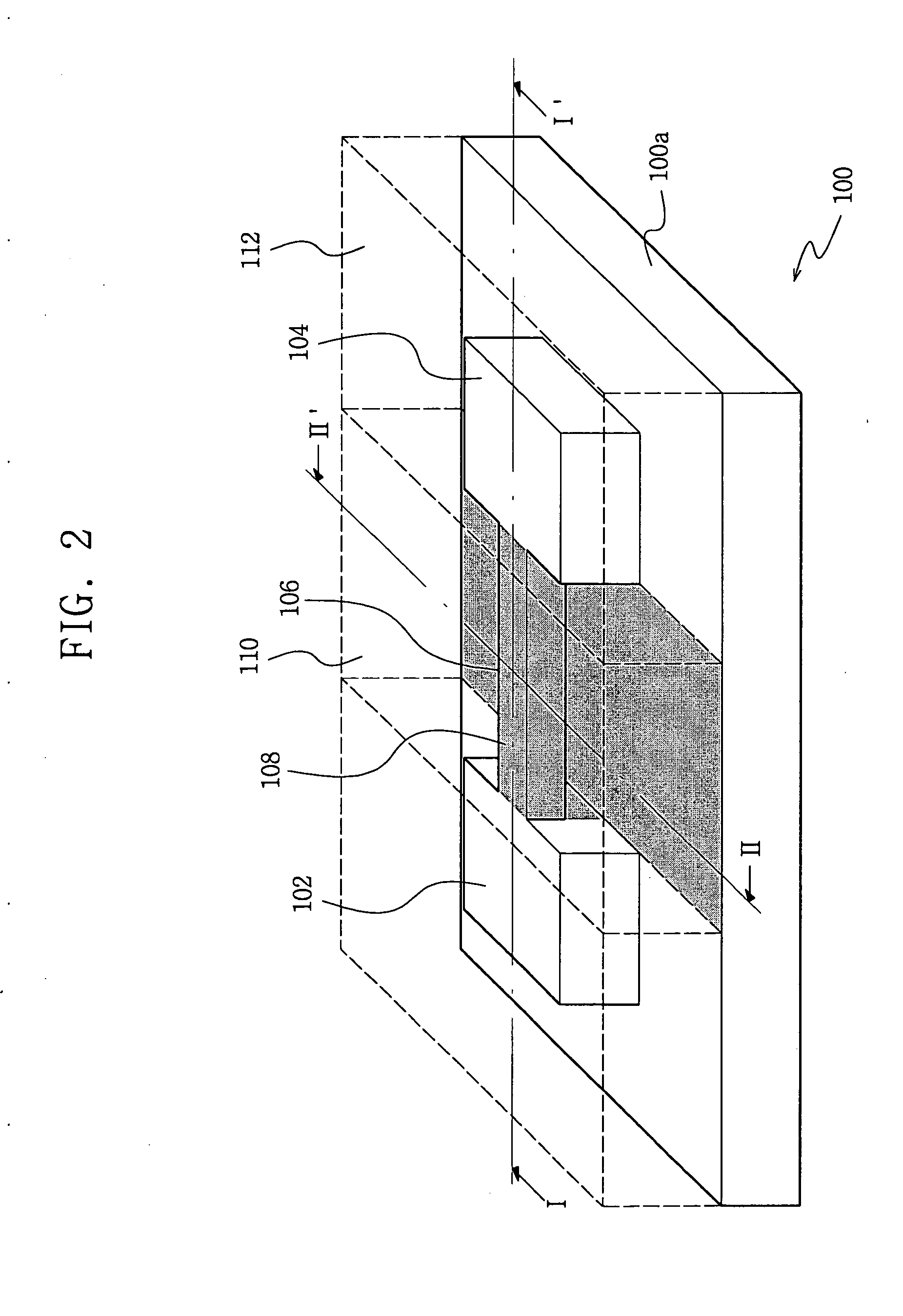
[0029]FIG. 2 is a perspective view illustrating a field effect transistor according to an exemplary embodiment of the invention.

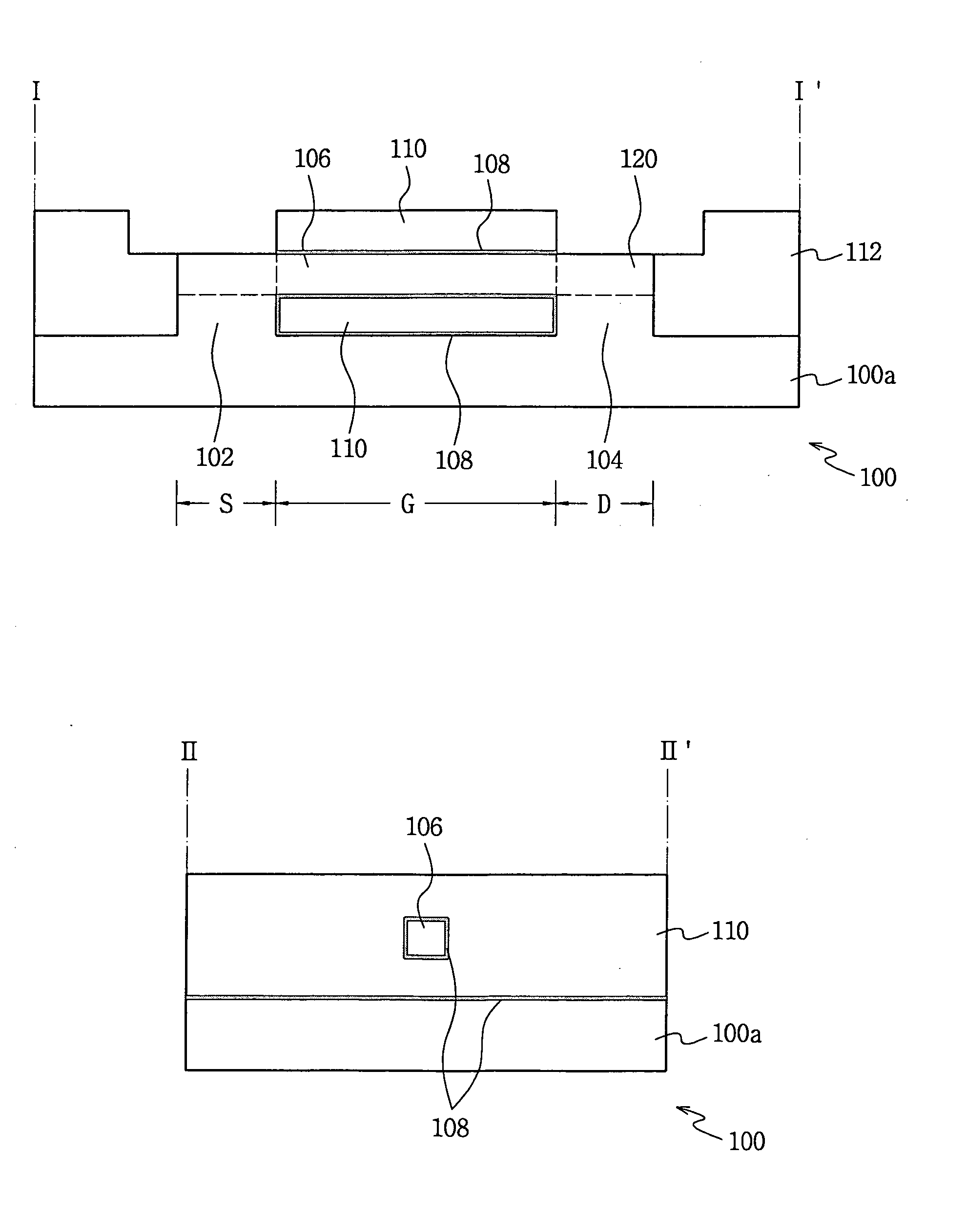
[0030] Referring to FIG. 2, according to the exemplary embodiment, first and second active regions 102 and 104 are distanced from each other and protrude from an upper surface of a lower layer of a semiconductor substrate 100. The se...


PUM


Abstract

In one embodiment, a semiconductor device includes a semiconductor substrate having a lower layer and an upper layer overlying the lower layer. The upper layer is arranged and structured to form first and second active regions that are spaced apart from each other and protrude from an upper surface of the lower layer. A third active region of a bridge shape is distanced vertically from the upper surface of the lower layer and connects the first and second active regions. The device further includes a gate electrode, which is formed with a gate insulation layer surrounding the third active region, so that the third active region functions as a channel.

Description

CROSS REFERENCE TO RELATED APPLICATIONS [0001] This application claims priority from Korean Patent Application No. 2004-8590, filed on Feb. 10, 2004, the contents of which are hereby incorporated by reference for all purposes. BACKGROUND OF THE INVENTION [0002] 1. Field of the Invention [0003] This disclosure relates to a semiconductor device, and more particularly, to a field effect transistor having a gate all around (GAA) structure and a method of manufacturing the same. [0004] 2. Description of the Related Art [0005] A recent rapid development in the information and communication fields, and a popularization of information media, such as computers, have brought rapid progress of semiconductor devices. A high-integration of semiconductor devices has brought about research for several kinds of methods to reduce a feature size of individual devices formed on a substrate from a functional viewpoint, and to increase performance of the devices. In such methods a field effect transisto...

Claims


Application Information

Patent Timeline
Patent Type & Authority Applications(United States)
IPC IPC(8): B82Y10/00H01L21/00H01L21/336H01L21/8234H01L21/84H01L27/08H01L27/088H01L21/28H01L27/092H01L29/423H01L29/49H01L29/76H01L29/78H01L29/786H01L29/94H01L31/062H01L31/113H01L31/119
CPCH01L29/42384H01L29/42392H01L29/66772H01L29/78648H01L29/7854H01L29/78603H01L29/785G07F9/10G07F11/20G07F17/0071
Inventor LEE, CHOONG-HOYOON, JAE-MANPARK, DONG-GUNLEE, CHUL
Owner SAMSUNG ELECTRONICS CO LTD
Why Eureka
Try Eureka