Semiconductor device and display comprising same
a technology of semiconductor devices and displays, applied in semiconductor devices, semiconductor/solid-state device details, electrical apparatus, etc., can solve problems such as inability to obtain performance, and achieve the effect of improving performance and versatile techniqu
- Summary
- Abstract
- Description
- Claims
- Application Information
AI Technical Summary
Benefits of technology
Problems solved by technology
Method used
Image
Examples
first embodiment
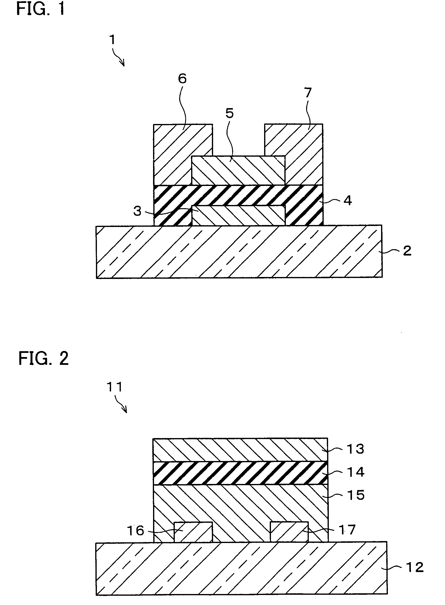
[0039] The following description discusses an embodiment of the present invention with reference to FIG. 1.
[0040]FIG. 1 is a cross sectional view illustrating a structure of a field effect transistor (FET) 1, which is a semiconductor apparatus of an embodiment of the present invention. The FET 1 is an inverse-staggered MOSFET (metal oxide semiconductor field effect transistor). Schematically, in the FET 1, a gate layer 3, a gate insulating layer 4, a channel layer 5 are layered on a substrate 2 in this order. And then, a source layer 6 and a drain layer 7 are layered thereon.
[0041] The substrate 2 serves as a base on which the layers are provided. A material of the substrate 2 may be silicon wafer, glass, plastic, or the like, and is not particularly limited in the present invention. The gate layer 3 is a gate wire for driving the FET 1, and a material of the gate layer 3 is a conductive material such as metal, semiconductor, or the like, and is not particularly limited. Normally,...
second embodiment
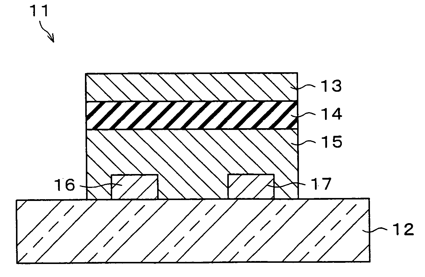
[0056] The following description discusses another embodiment of the present invention with reference to FIG. 2.
[0057]FIG. 2 is a cross sectional view illustrating a structure of an FET 11, which is a semiconductor apparatus of the another embodiment of the present invention. The FET 11 is a staggered MOSFET. Schematically, in the FET 11, a source layer 16 and a drain layer 17 are layered on a substrate 12. Then, a channel layer 15, a gate insulating layer 14, and a gate layer 13 are layered in this order on them formed on the substrate 12. The substrate 12 and the layers 13 through 17 have equivalent functions, materials, and thickness to the substrate 2 and the layers 3 through 7 in the FET 1 (see FIG. 1), respectively. Therefore, explanations of them are omitted here.
[0058] Apparently from a comparison between the structures of FIG. 1 and FIG. 2, either the gate insulating layers 4 and 14 or the channel layers 5 and 15 can be firstly formed. This ensures more freedom in designi...
third embodiment
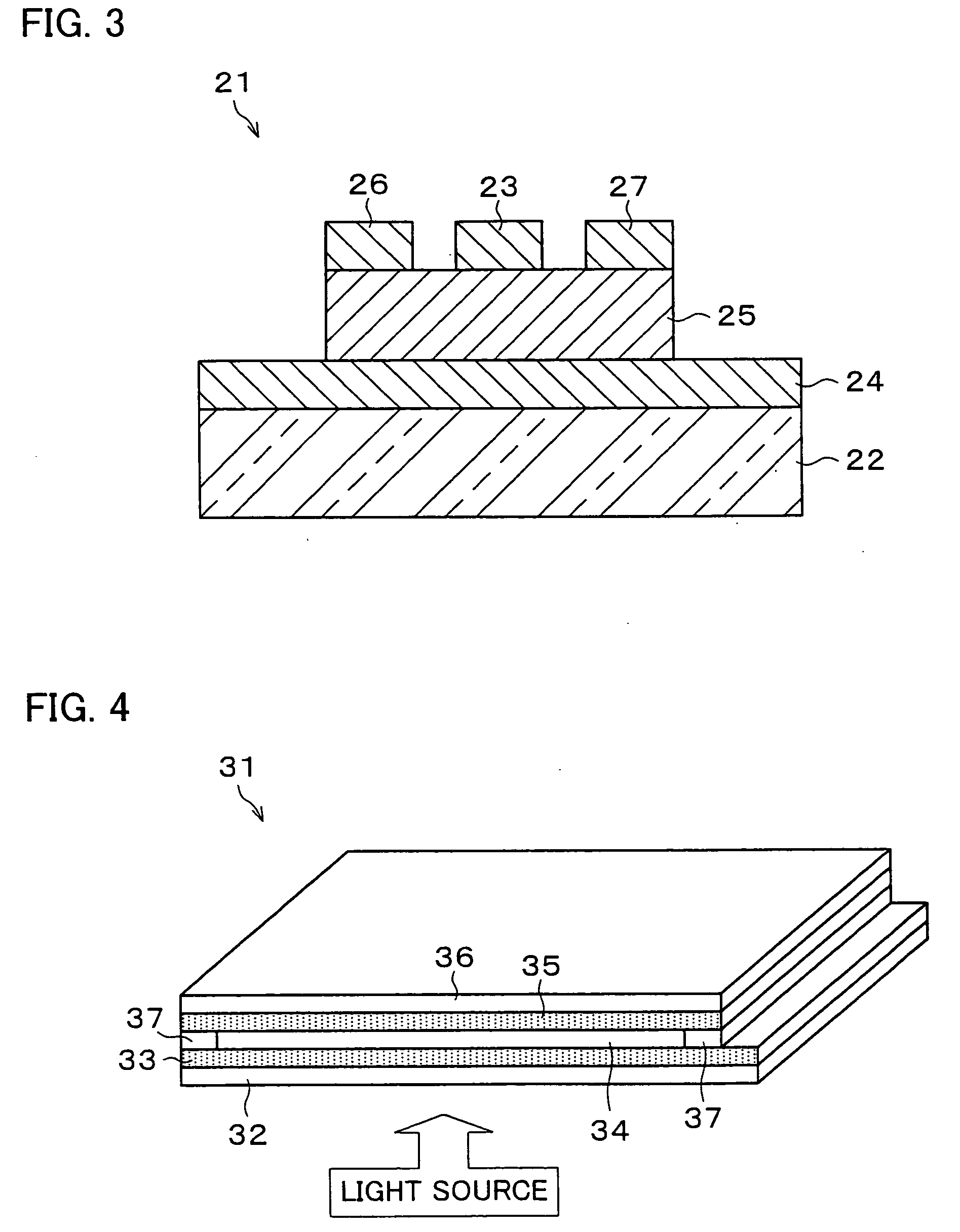
[0060] The following description discusses still another embodiment of the present invention with reference to FIG. 3.
[0061]FIG. 3 is a cross sectional view illustrating a structure of FET 21, which is a semiconductor apparatus of the still another embodiment of the present invention. The FET 21 is a Schottky-gate FET. Schematically, in the FET 21, a priming layer 24, and a channel layer 25 are layered on a substrate 22 in this order. Further, a gate layer 23, a source layer 26 and a drain layer 27 are layered on the channel layer 25.
[0062] Like the substrates 2 and 12, the substrate 22 serves as a base for mounting the layers 23 through 27 thereon. A material of the substrate 22 is not particularly limited in the present invention, and may be silicon wafer, glass, plastic, or the like. As described above, in the case where the priming layer 24 is formed on the substrate 22, the substrate 22 normally has a film thickness not less than 0.1 mm but not more than 2 mm, however, the fi...
PUM
 Abstract
Description
Claims
Application Information
 - R&D
- Intellectual Property
- Life Sciences
- Materials
- Tech Scout
- Unparalleled Data Quality
- Higher Quality Content
- 60% Fewer Hallucinations
Browse by: Latest US Patents, China's latest patents, Technical Efficacy Thesaurus, Application Domain, Technology Topic, Popular Technical Reports.
© 2025 PatSnap. All rights reserved.Legal|Privacy policy|Modern Slavery Act Transparency Statement|Sitemap|About US| Contact US: help@patsnap.com


