Memory system and method for assigning addresses to memory devices

a memory device and address technology, applied in the field of memory systems, can solve the problems of large memory boards and relatively large pin count of control logic circuitry, unsatisfactory radial device selection approach of fig. 1, and distinct possibility of error

Inactive Publication Date: 2005-07-21
MICRON TECH INC
View PDF19 Cites 23 Cited by
  • Summary
  • Abstract
  • Description
  • Claims
  • Application Information

AI Technical Summary

Problems solved by technology

However, if a large number of memory devices are used so that large amounts of data can be stored, the requirement of separate select lines for each memory device results in large memory boards and a relatively large pin count for the control logic circuitry.
Thus, unless access speed is critical and a large number of memory devices are used, the radial device selection approach of FIG. 1 is not ideal.
Thus, there is a distinct possibility for error.
These pins increase the pin count for the integrated circuits thereby increasing the cost of the packaging for the devices and increasing the likelihood that there will be mechanical problems and manufacturing errors through soldering and the like.
These extra pins are also subject to defects and increase the possibility of damage to the integrated circuits as a result of electrostatic discharge.

Method used


Image

  • Memory system and method for assigning addresses to memory devices
  • Memory system and method for assigning addresses to memory devices
  • Memory system and method for assigning addresses to memory devices

Examples


Embodiment Construction

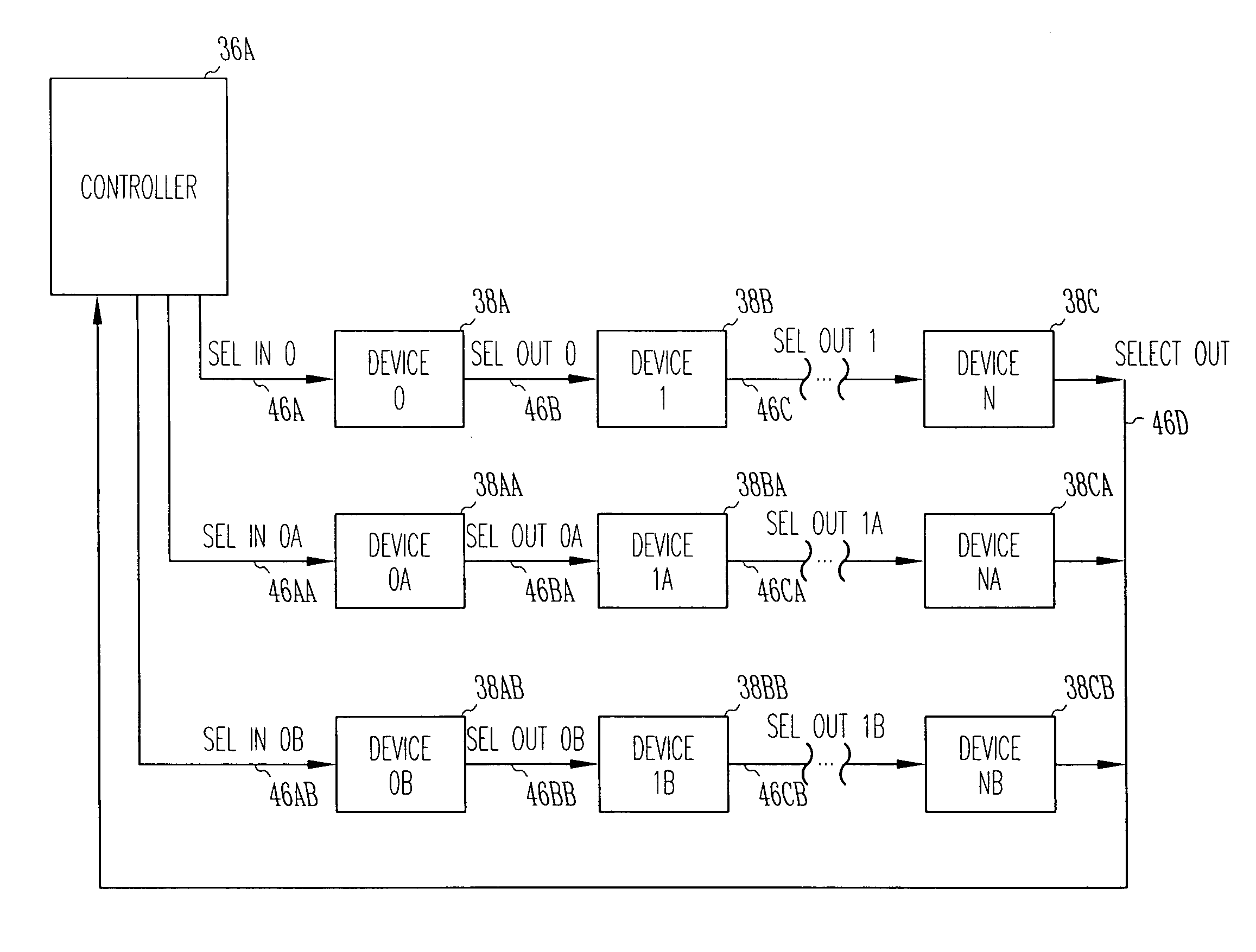
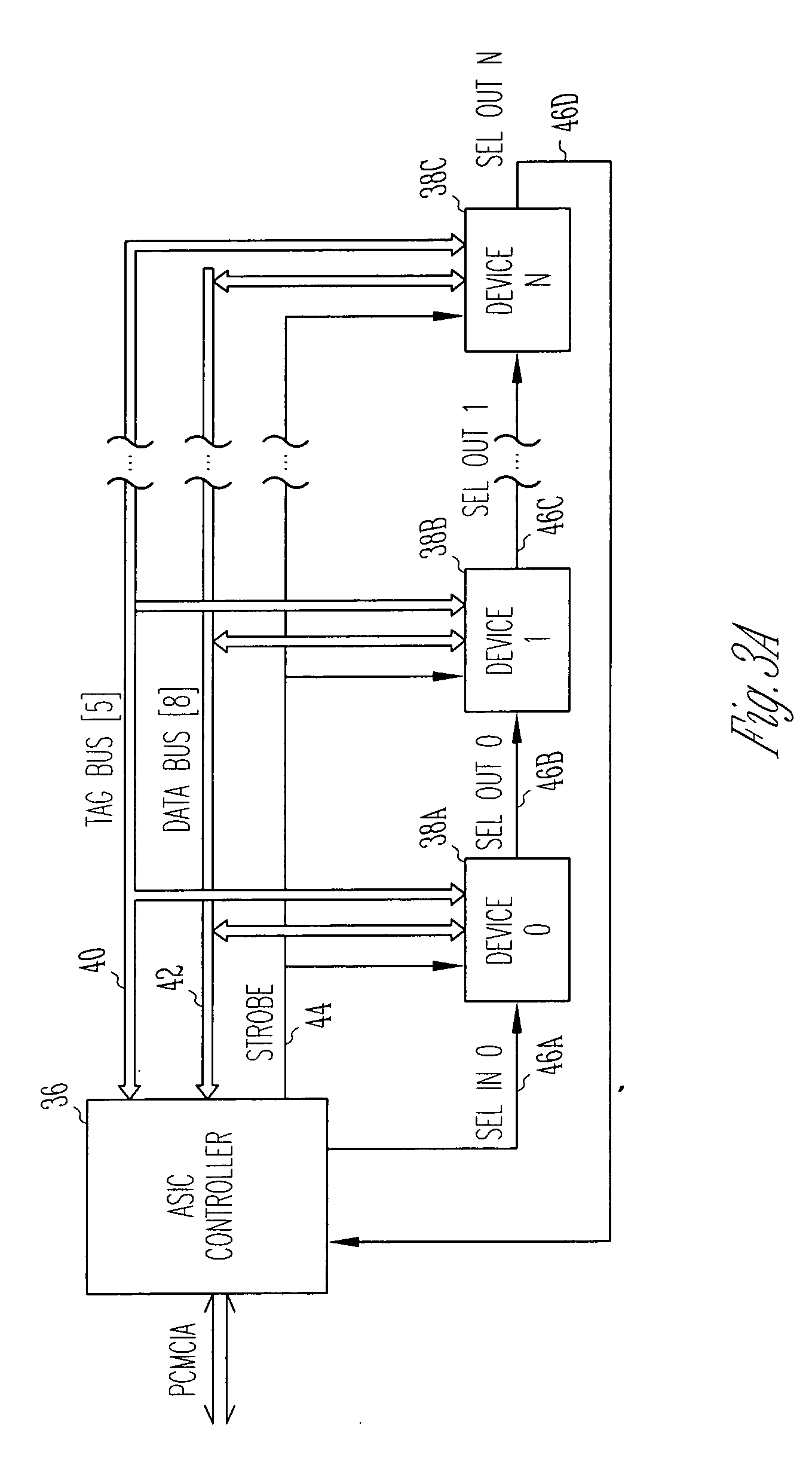
[0043] Referring again to the drawings, FIG. 3A is a simplified block diagram of an embodiment of a memory system in accordance with the present invention. The exemplary memory system to be described is a mass storage memory system used to emulate the operation of a hard disc drive. It should be noted, however, that the subject invention is suitable for use in a large variety of other applications.

[0044] The memory system includes a Controller 36 and a plurality of memory devices 38A, 38B and 38C. The Controller 36 can be implemented using a wide variety of techniques including ASIC (Application Specific Integrated Circuit) technology. The Controller 36 is best understood by describing its functionality, with the particular implementation forming no part of the present invention. Since the Controller can be readily constructed by persons of ordinary skill in the art based upon the following functional description, details regarding a particular implementation will not be provided s...


PUM


Abstract

A memory system having a memory controller and several separate memory devices connected to the controller by a system bus. The memory devices each included an array of memory cells, addressing circuitry used to address the cells and an address storage circuit which stores a local address unique to each of the memory devices. The local addresses are sequentially assigned to the memory devices by selecting a first one of the devices and forwarding an address assign command to the selected device. A command decoder, having detected the address assign command, will permit a local address placed on the bus by the controller to be loaded into the selected memory device. This sequence will continue until all of the memory devices have been assigned local addresses at which time the memory devices can be accessed to perform memory read, program, erase and other operations.

Description

BACKGROUND OF THE INVENTION [0001] 1. Field of the Invention [0002] The present invention relates generally to memory systems and in particular to memory systems having multiple memory devices and a controller for serial selection of the memory devices. [0003] 2. Description of Related Art [0004] Data systems incorporating memory systems having multiple memory devices are well known. By way of example, FIG. 1 depicts a simplified conventional memory system which includes a host device 20, an address decoder 22 and memory devices 24A and 24B. The host device 22 may be a microprocessor and the memory devices 24A and 24B may be separate memory integrated circuits. An address bus 26 is used to provide addresses to an address decoder 22 and to the memory devices 24A and 24B. The address decoder 22 has two outputs connected to enable inputs of the memory devices 24A and 24B. Typically, the most significant bit(s) of the address are provided on the bus 26 to the decoder 22, with the remain...

Claims


Application Information

Patent Timeline
Patent Type & Authority Applications(United States)
IPC IPC(8): G06F12/06
CPCG06F13/1694G06F12/0661
Inventor NORMAN, ROBERT D.LAKHANI, VINOD C.
Owner MICRON TECH INC
Why Eureka
Try Eureka