Storage device and method

a technology of storage devices and storage devices, applied in the field of storage devices, can solve the problems of high resolution required, serious constraints in implementing an active servo control with reasonable speed, and limiting the data rate to rather low values

Inactive Publication Date: 2005-07-21
IBM CORP
View PDF15 Cites 13 Cited by
  • Summary
  • Abstract
  • Description
  • Claims
  • Application Information

AI Technical Summary

Problems solved by technology

These characteristics impose serious constraints in implementing an active servo control with reasonable speed.
The low tunnelling currents and feedback speed limit the data rate to rather low values.
Thus, one of the most critical issues in detecting the presence or absence of an indentation is the high resolution required to extract the signal that contains the information about the logical bit being “1” or “0”.
Sensitivity, power consumption, and size are critical issues for all aforementioned integrated sensing or read back approaches.
For example, in piezoresistive sensing the main issues are the size of the sensor and its sensitivity in terms of the variation of the electrical resistance expressed as ΔR / R.
Similarly, in Millipede, the main issues with thermomechanical or thermal sensing are power consumption, sensitivity in terms of variation of the thermal resistance and limitation on the data rate per lever due to the thermal time constant of the lever.
Due to limitations regarding the data rate of a single cantilever, massive parallelization is needed to achieve high data rates.
However, this approach has the disadvantages of limitations of single AFM sensors regarding sensitivity, power consumption, and read back data rate associated with previous approaches.
However, the capacitance between the conductive tip and the surface of the sample is not constant.
Additionally, the configuration is extremely difficult to implement in parallel operation which is required in probe-storage applications.

Method used


Image

  • Storage device and method
  • Storage device and method
  • Storage device and method

Examples


Embodiment Construction

[0024] An embodiment of the invention applies capacitive read-out to scanning probes, where optical, piezoresistive, or thermal read-out techniques are often used, for example, for sensing or reading back stored information in polymer media using a single sensor (cantilever) or a plurality of sensors (cantilevers) in a 2-D arrangement.

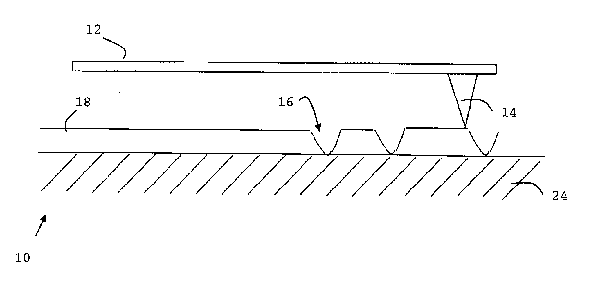
[0025]FIG. 1 shows the cross-section of a general probe-based storage device. The device comprises a scanning lever 12 such as a spring cantilever having a tip 14 at one end of the lever. The scanning lever is arranged to be sensitive to vertical forces, and contact a sample 18 such as a polymer media on a conducting substrate 24. The sample may have indentations 16 or marks that the tip of the lever traverses.

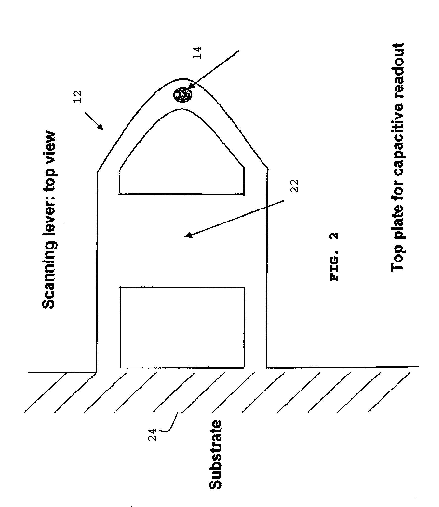
[0026]FIG. 2 shows the top plan view of a two-terminal probe or lever 12 in accordance with an embodiment of the invention that has the desired properties for capacitive sensing. The lever comprises the tip 14, and a capacitive platform 22 for ...


PUM

PropertyMeasurementUnit
capacitanceaaaaaaaaaa
structureaaaaaaaaaa
AFMaaaaaaaaaa

Abstract

A storage device is provided, comprising of a storage surface having perturbations representative of information stored in the storage device; a lever having at least one tip facing the storage surface and movable substantially parallel thereto; and a variable capacitor having a first plate and a second plate, the first plate being integral to the storage surface and the second plate being integral to the lever, wherein movement of the lever relative to the surface produces variation in the capacitance of the variable capacitor in response to the tip scanning across the perturbations of the surface.

Description

FIELD OF THE INVENTION [0001] This invention relates to storage devices, and more particularly, this invention relates to probe-based storage devices. BACKGROUND OF THE INVENTION [0002] In the field of this invention techniques are known that use nanometer-sharp tips for imaging and investigating the structure of materials down to the atomic scale. Such techniques include scanning tunnelling microscopy (STM) and atomic force microscopy (AFM), as described in Binnig, G. et al., “7×7 reconstruction on Si(111) resolved in real space,” Phys. Rev. Lett., 50 (1983) 120 (Binnig 1983); and Binnig, G. et al., “Atomic force microscope,” Phys. Rev. Lett., 56 (1986) 930 (Binnig 1986). Both STM and AFM are suitable for the development of ultrahigh-density storage devices, as discussed in U.S. Pat. No. 4,575,822 issued 11 Mar. 1986 to Quate, which discloses a digital memory in which data is stored by establishing perturbations in the surface of a substrate and thereafter identifying the perturbat...

Claims


Application Information

Patent Timeline
Patent Type & Authority Applications(United States)
IPC IPC(8): G11B9/00G11B11/00G11C7/00
CPCB82Y10/00G11B11/007G11B9/149
Inventor BINNIG, GERD K.ELEFTHERIOU, EVANGELOS S.HAGLEITNER, CHRISTOPH
Owner IBM CORP
Why Eureka
Try Eureka