
Data processing device and method utilizing latency difference between memory blocks

Inactive Publication Date: 2005-06-30
FUJITSU LTD
View PDF7 Cites 10 Cited by
  • Summary
  • Abstract
  • Description
  • Claims
  • Application Information

AI Technical Summary

Benefits of technology

[0022] It is an object of the present invention to provide a data processing device for improving memory access speed when large-capacity memory is mounted on a semiconductor integrated circuit, such as an LSI, and a method thereof.

Problems solved by technology

(2) Conventionally, a ratio of wiring delay time to the entire delay time in an LSI is small, and delay is mainly caused by gate delay time.
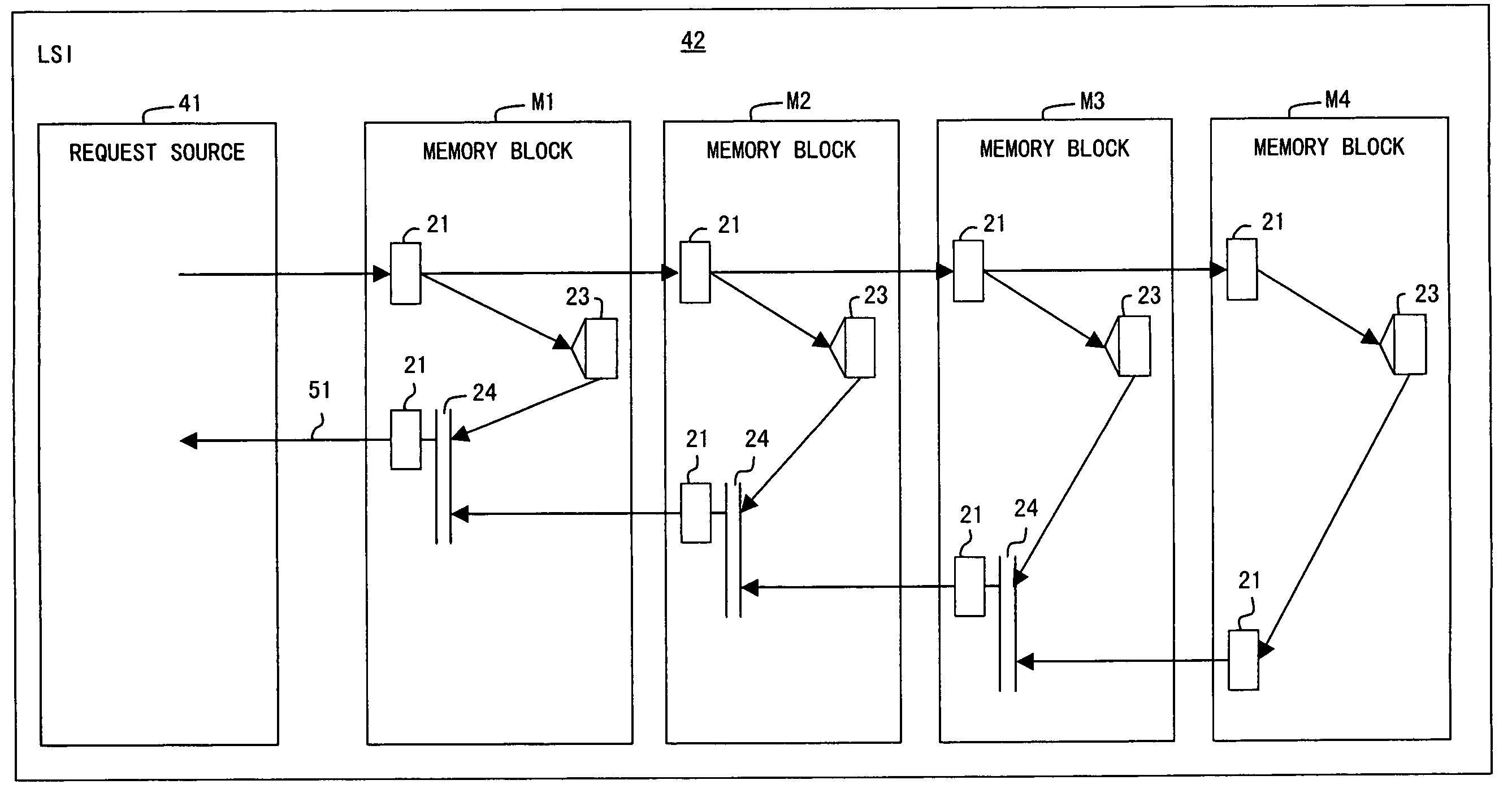
However, as with the advancement of the processing technology of semiconductors, the speed (clock frequency) of an LSI has further improved, the wiring delay time in an LSI has become dominant, and delay difference due to a difference in a position disposed in an LSI between the two segments of memory cannot be negligible.
If in such a state, control is performed by single latency as ever, as a result, a wiring delay time obtained when the farthest memory is accessed cannot be helped being adopted.
In that case, the latency of memory access becomes very long to affect process performance.
Therefore, the process of a request to memory blocks other than M4 greatly delays.

Method used


Image

  • Data processing device and method utilizing latency difference between memory blocks
  • Data processing device and method utilizing latency difference between memory blocks
  • Data processing device and method utilizing latency difference between memory blocks

Examples


Embodiment Construction

[0052] The preferred embodiments of the present invention are described in detail below with reference to the drawings.

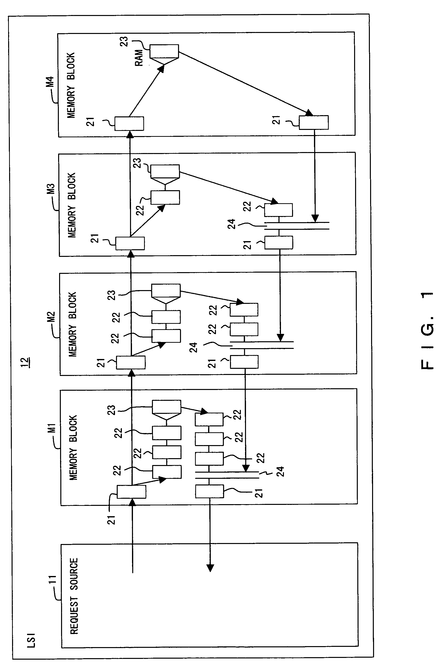
[0053] In this preferred embodiment, memory in an LSI is divided into a plurality of blocks according to a latency difference so that a result can be returned to an access to a block with short latency (block located physically close to a request source). Thus, average latency is shortened by effectively using a latency difference, and accordingly, the performance of an LSI can be improved.

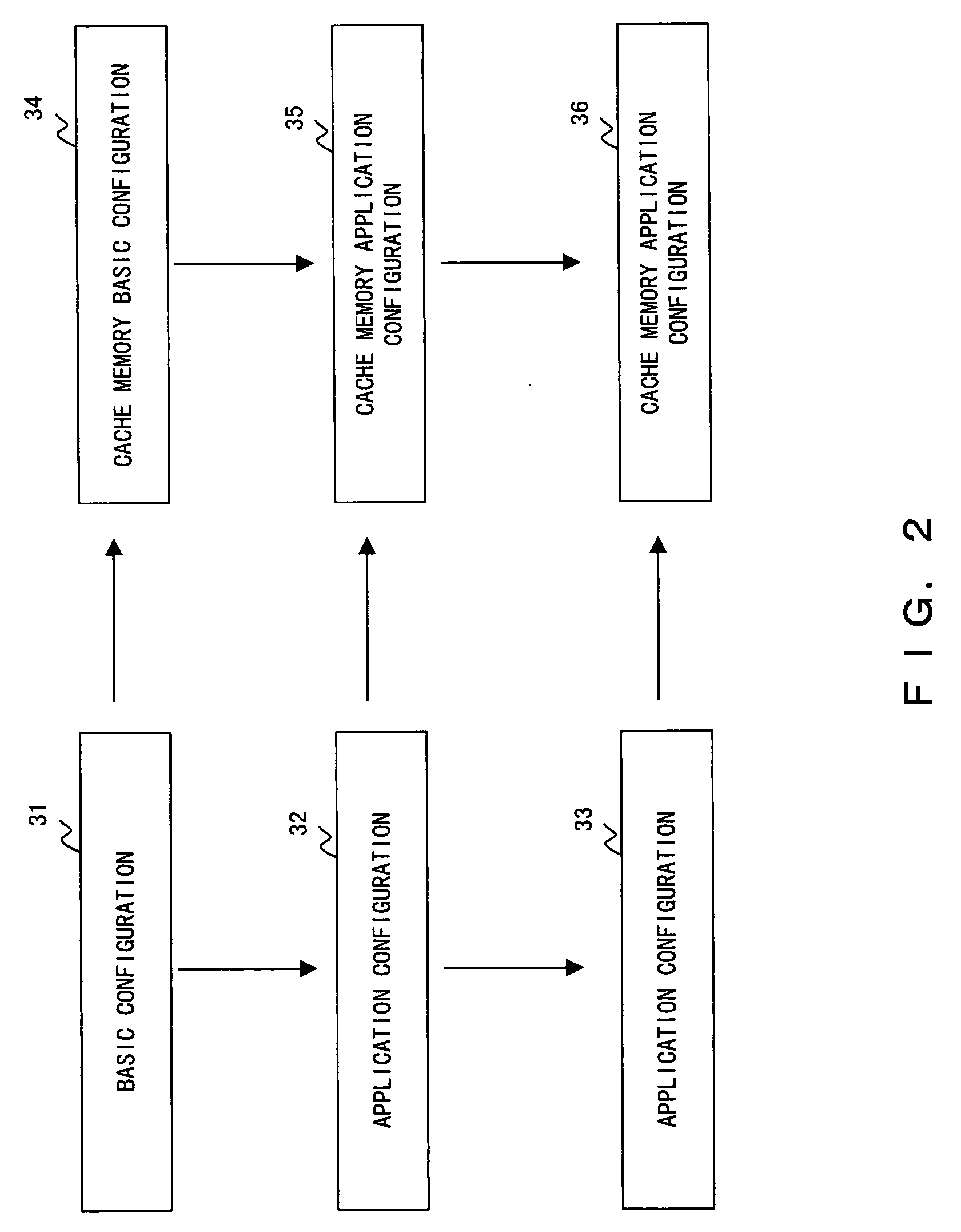
[0054] The configuration of the data processing device in this preferred embodiment can be largely classified into six configurations as shown in FIG. 2. A basic configuration 31 takes into consideration the relationship between the position of a request source and the position of data disposed in memory, and the data in the memory is divided into blocks according to a latency difference. An application configuration 32 can be obtained by adding one step of a variable-length buf...


PUM


Abstract

Each of a plurality of memory blocks returns data in different latency in reply to a data request from a request source. The closer a request destination memory block is to the request source, in the shorter latency the data is returned.

Description

CROSS-REFERENCE TO RELATED APPLICATION [0001] This is a continuation of an International Application No. PCT / JP02 / 09290, which was filed on Sep. 11, 2002.BACKGROUND OF THE INVENTION [0002] 1. Field of the Invention [0003] The present invention relates to a data processing device with memory composed of a plurality of blocks, and a method thereof for processing such memory data. [0004] 2. Description of the Related Art [0005] Improvement in both the degree of integration and speed of large-scale integrated circuits (LSI), including micro-processors is remarkable. With the high speed of an LSI, its difference with external memory, such as a main storage and like has increased. In order to fill in up the difference, a method for mounting a cache memory with a large capacity (that is, a large area) on an LSI has become popular. [0006] In small devices requiring data processing capability, including a cellular phone and a personal digital assistance (PDA), a processor and a main storage ...

Claims


Application Information

Patent Timeline
IPC IPC(8): G06F12/00G06F13/42
CPCG06F13/4243
Inventor NODOMI, AKIRANAKADA, TATSUMIITO, EIKISAKATA, HIDEKI
Owner FUJITSU LTD
Learn More