Gas assisted method for applying resist stripper and gas-resist stripper combinations

a technology of resist stripper and gas assisted method, which is applied in the direction of photomechanical equipment, instruments, and cleaning using liquids, etc., can solve the problems of ozonated water resist stripper losing its effectiveness, reducing the efficiency of resist stripper, and reducing the rate at which resist stripper removes photoresist from the semiconductor device structure, so as to prevent the stagnation the effect of increasing the rate of resist stripper and preventing the reduction of the ra

Inactive Publication Date: 2005-06-02
OVONYX MEMORY TECH LLC
View PDF14 Cites 1 Cited by
  • Summary
  • Abstract
  • Description
  • Claims
  • Application Information

AI Technical Summary

Benefits of technology

[0016] The resist stripper may be exposed to one or more gases or other carrier fluids prior to, during, or after application thereof onto a photoresist on the semiconductor device structure. The one or more other, non-ozone gases may thin the layer of resist stripper over the semiconductor device structure or move the resist stripper across a surface of the semiconductor device structure, both of which prevent the formation of or eliminate macroscopic drops of resist stripper on the semiconductor device structure. Alternatively, the one or more gases may be the product of one or more chemical reactions effected by or in the resist stripper, in which case the one or more gases are formed in the resist stripper. In any event, by exposing the resist stripper to one or more gases or other carrier fluids, the rate at which the resist stripper removes photoresist from the semiconductor device structure is increased.
[0017] As an example of the manner in which resist stripper may be moved across the surface of the semiconductor device structure, one or more gases under pressure, such as in a jet or stream of liquid or gas, may be directed at least partially across the surface of the semiconductor device structure so as to force resist stripper across the semiconductor device structure. This movement of resist stripper across the surface of the substrate prevents stagnation of the resist stripper and, consequently, prevents a reduction in the rate at which the resist stripper removes the photomask from the semiconductor substrate.
[0019] The one or more gases may be directed across the surface of the semiconductor device structure from a central region thereof toward an outer periphery thereof. Alternatively, the one or more gases may be directed onto a surface of a semiconductor device structure near a peripheral edge thereof so as to move resist stripper across the semiconductor device structure. Application of one or more gases may also be effected in any alternative manner that facilitates the substantially continuous movement of resist stripper across the surface of the semiconductor device structure.

Problems solved by technology

Thus, the concentrations of active chemicals in these wet chemical resist strippers decrease over time, thereby reducing the effectiveness of these resist strippers.
Thus, ozonated water resist strippers lose their effectiveness over time.
Conventional processes for applying resist strippers to resist, such as spraying or immersion, do not facilitate continuous movement of the resist strippers across the semiconductor device structure following application and may, therefore, permit the resist strippers to sit, or stagnate, on the resist.
Stagnation of resist strippers is somewhat undesirable, however, as the concentrations of reaction products may increase during stagnation and stagnation may, therefore, reduce the rate at which the resist strippers remove photomasks from semiconductor device structures.
The art lacks teaching of methods for introducing one or more gases into or onto a resist stripper to maintain a desired rate for stripping resist from a semiconductor device structure, as well as stripping systems for effecting such methods.

Method used


Image

  • Gas assisted method for applying resist stripper and gas-resist stripper combinations
  • Gas assisted method for applying resist stripper and gas-resist stripper combinations
  • Gas assisted method for applying resist stripper and gas-resist stripper combinations

Examples


Embodiment Construction

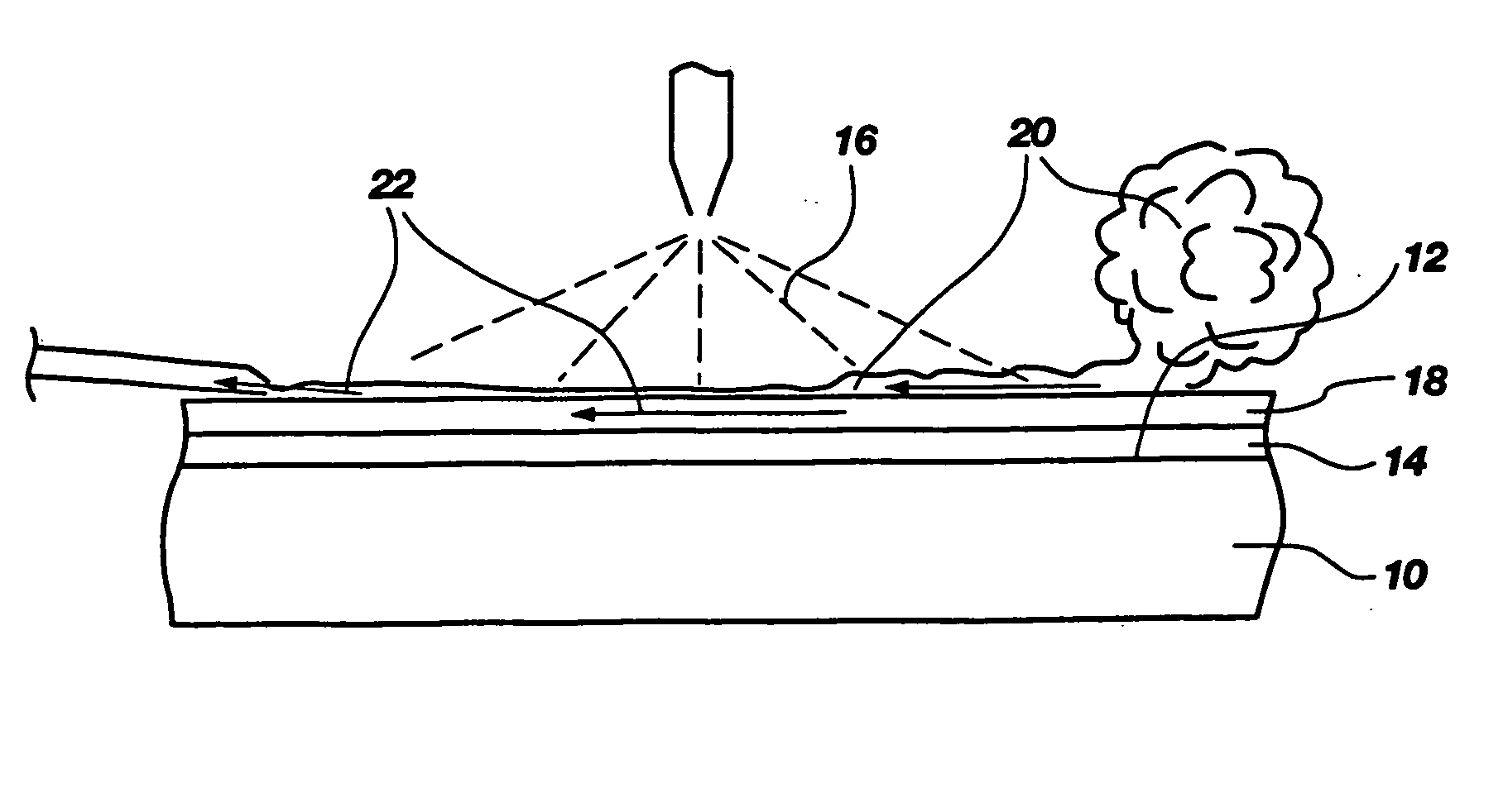
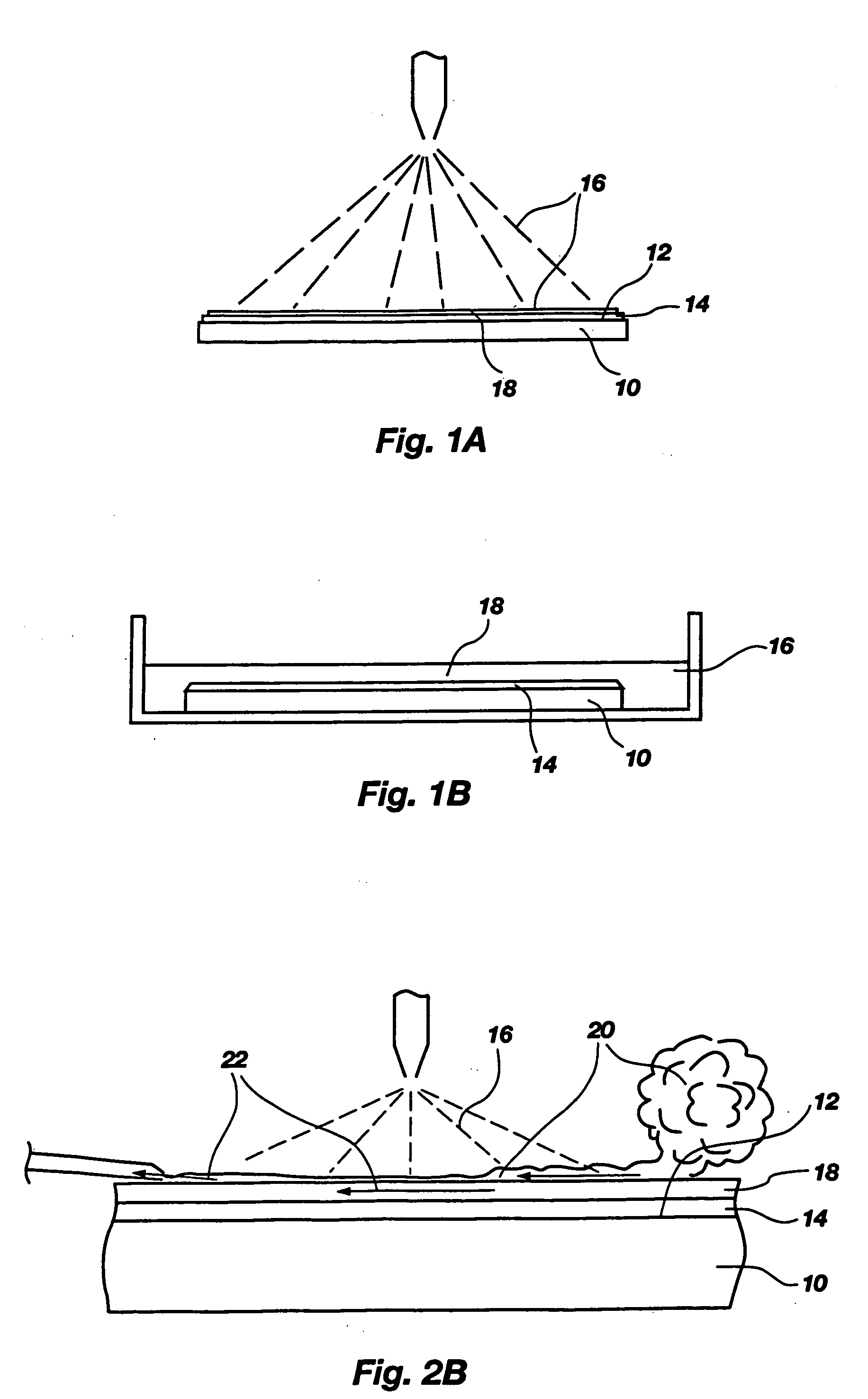
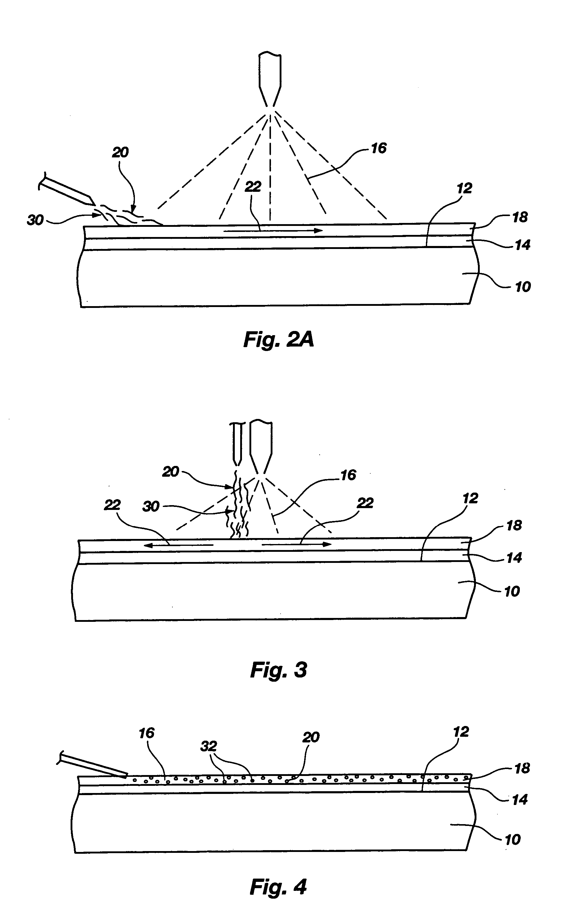
[0031]FIG. 1A schematically illustrates a semiconductor device structure 10, in this case a semiconductor wafer, including a photomask 14 over an active surface 12 thereof. Photomask 14 is formed from polymerized, or consolidated, photoresist and may be either soft-baked or hard-baked, as known in the art. Resist stripper 16 preferably includes ozone (e.g., ozonated water), but may be any other type of resist stripper known and used in the art. Resist stripper 16 may be applied to photomask 14 by known processes, such as by spraying resist stripper 16 onto photomask 14, as shown in FIG. 1A. As an alternative, resist stripper 16 may be applied to photomask 14 by at least partially immersing photomask 14 in a quantity of resist stripper 16, as illustrated in FIG. 1B. In any event, resist stripper 16 forms a layer 18 over semiconductor device structure 10 and over any photomask 14 on active surface 12 of semiconductor device structure 10.

[0032] In order to effect the method of the pre...


PUM

PropertyMeasurementUnit
movementaaaaaaaaaa
electrically conductiveaaaaaaaaaa
semiconductiveaaaaaaaaaa

Abstract

A method for moving resist stripper across the surface of a semiconductor substrate that includes applying a wet chemical resist stripper, such as an organic or oxidizing wet chemical resist stripper, to at least a portion of a photomask positioned over the semiconductor substrate. A carrier fluid, such as a gas, is then directed toward the semiconductor substrate so as to move the resist stripper across the substrate. The carrier fluid may be directed toward the substrate as the resist stripper is being applied thereto or following application of the resist stripper. A system for effecting the method is also disclosed.

Description

CROSS-REFERENCE TO RELATED APPLICATIONS [0001] This application is a continuation of application Ser. No. 10 / 164,431, filed Jun. 6, 2002, pending, which is a continuation of application Ser. No. 09 / 639,550, filed Aug. 16, 2000, now U.S. Pat. No. 6,440,871, issued Aug. 27, 2002.BACKGROUND OF THE INVENTION [0002] 1. Field of the Invention [0003] The present invention relates generally to methods for stripping photoresist from a semiconductor device structure and, in particular, to methods for continuously moving resist stripper across the surface of a semiconductor device structure. More particularly, the present invention relates to resist stripper application methods that include exposing the resist stripper to a gas, to move the resist stripper across the semiconductor device structure, to thin the resist stripper, or to otherwise increase the rate at which the resist stripper removes photoresist from the semiconductor device structure. [0004] 2. Background of Related Art [0005] In...

Claims


Application Information

Patent Timeline
Patent Type & Authority Applications(United States)
IPC IPC(8): B05D1/00B08B3/00C03C15/00G03F7/42H01L21/00H01L21/302H01L21/306H01L21/311H01L21/338H01L21/461
CPCG03F7/423G03F7/427H01L21/02054Y10S438/948H01L21/6708H01L21/6715H01L21/31133
Inventor GILTON, TERRY L.
Owner OVONYX MEMORY TECH LLC
Why Eureka
Try Eureka