
Method for monitoring a batch system

a batch system and batch technology, applied in semiconductor/solid-state device testing/measurement, semiconductor/solid-state device details, instruments, etc., can solve problems such as and achieve the effect of reducing financial, logistical and fabrication-based expenditur

Inactive Publication Date: 2005-04-28
INFINEON TECH AG
View PDF10 Cites 1 Cited by
  • Summary
  • Abstract
  • Description
  • Claims
  • Application Information

AI Technical Summary

Benefits of technology

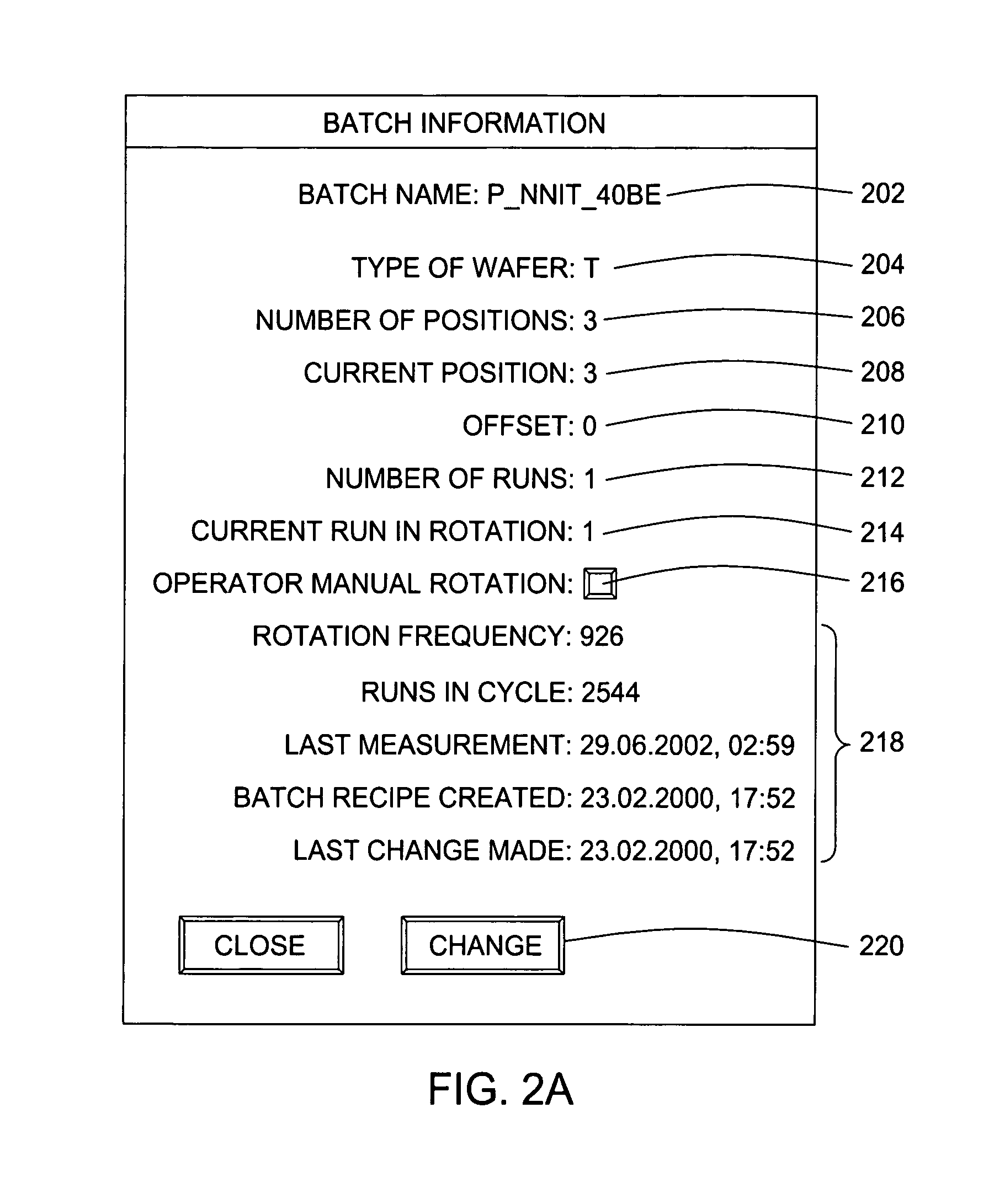
The invention provides a method for monitoring batch systems with reduced expenditure. The method involves rotating test wafers in a boat during specific passes of the batch system and measuring them afterward to assess the condition of the system and the quality of the production process. The method allows for reliable monitoring with a reduction in the number of test wafers needed and effort required by fabrication personnel. The rotation of the test wafers is achieved by changing the load pattern without affecting the fabrication process. A user interface is provided to define parameters for the test wafer rotation, and a log mechanism is used to diagnose errors and track changes in the load pattern.

Problems solved by technology

However, the necessary comprehensive wafer inspections lead to a considerable financial, logistic and fabrication-based expenditure.

Method used


Image

  • Method for monitoring a batch system
  • Method for monitoring a batch system
  • Method for monitoring a batch system

Examples


Embodiment Construction

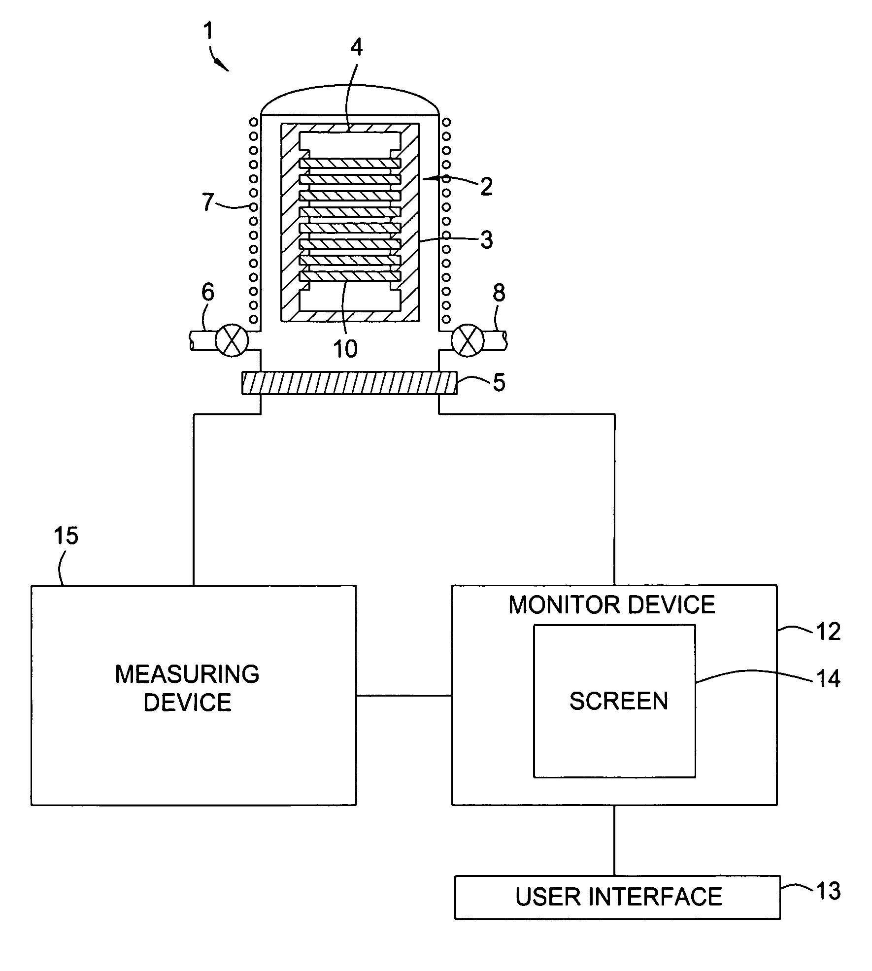
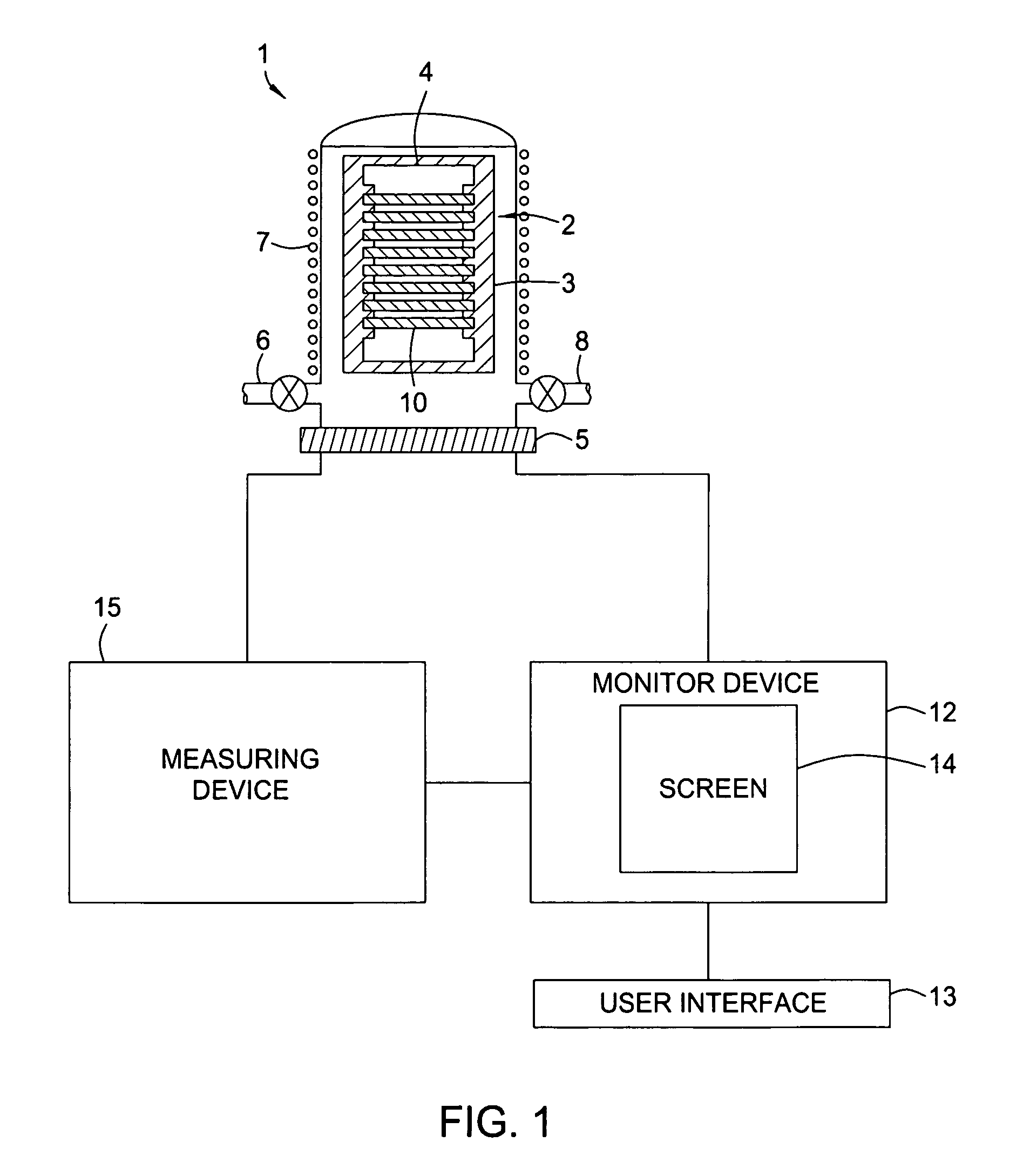
[0018]FIG. 1 shows a schematic sectional illustration through an LPCVD system for deposition of thin layers on semiconductor wafers. The method according to one embodiment of the invention for monitoring a batch system will be explained by way of example using such an LPCVD system. The method according to one embodiment of the invention may, however, be used in all other known batch systems in which a plurality of semiconductor wafers are processed simultaneously.

[0019] The LPCVD system shown in FIG. 1 comprises a process chamber 1, in which a carrier device 2, also designated a boat (used interchangeably herein), is arranged horizontally and is loaded with the semiconductor wafers 10 to be processed. The entirety of all the semiconductor wafers 10 loaded into the boat and to be processed simultaneously in the LPCVD system is called a load. The boat 2 has a frame comprising a plurality of rods 3 which are oriented in parallel and connected to one another by transverse struts 4. On ...


PUM

PropertyMeasurementUnit
volumeaaaaaaaaaa
temperaturesaaaaaaaaaa
pressureaaaaaaaaaa

Abstract

System and method for processing semiconductor wafers are provided. One embodiment provides a method for monitoring a batch system. For the purpose of monitoring batch systems, in accordance with a defined rotation principle, during successive passes of the batch system, a predefined number of test wafers is moved to changing positions in a boat, so that after a complete rotation cycle, in which test wafers and / or product wafers are inspected after specific passes, a statement about the condition of the batch system and the quality of the processing process is achieved.

Description

CROSS-REFERENCE TO RELATED APPLICATIONS [0001] This application claims foreign priority benefits under 35 U.S.C. §119 to co-pending German patent application number DE 103 40 511.9-33, filed Sep. 3, 2003. This related patent application is herein incorporated by reference in its entirety. BACKGROUND OF THE INVENTION [0002] 1. Field of the Invention [0003] The present invention relates to a system for monitoring a batch system. [0004] 2. Description of the Related Art [0005] During the processing of semiconductor wafers for the production of semiconductor components, use is preferably made of batch systems in which a plurality of semiconductor wafers can be processed simultaneously. The load, i.e., all the semiconductor wafers loaded into the batch system and to be processed, is in this case accommodated in a boat, i.e., an apparatus for holding the semiconductor wafers vertically or horizontally. [0006] The most important batch systems which are used in semiconductor technology incl...

Claims


Application Information

Patent Timeline
Patent Type & Authority Applications(United States)
IPC IPC(8): C23C16/52C23C16/54H01L21/66H01L23/544
CPCC23C16/52H01L22/34H01L22/20C23C16/54
Inventor RIEKER, NORMAN
Owner INFINEON TECH AG
Learn More