Nonvolatile semiconductor storage device

a semiconductor storage device and non-volatile technology, applied in the direction of digital storage, radio frequency controlled devices, instruments, etc., can solve the problems of increasing the number of man-hours, increasing the production cost of flash memory, and reducing efficiency

Inactive Publication Date: 2005-04-21
RENESAS ELECTRONICS CORP
View PDF1 Cites 24 Cited by
  • Summary
  • Abstract
  • Description
  • Claims
  • Application Information

AI Technical Summary

Benefits of technology

[0017] 7. In the above item 5 or 6, by the control signal that is delayed by the delay circuits, precharging bitlines of the memory banks when reading starts, delayed by a certain period of time after the start of precharging the preceding memory bank bitline.

Problems solved by technology

However, the present inventors found the following problems with the technique of programming the fuses of the flash memory to store the management information as mentioned above.
This results in a problem of increasing the number of man-hours and a decrease in efficiency.
This results in a problem o

Method used


Image

  • Nonvolatile semiconductor storage device
  • Nonvolatile semiconductor storage device
  • Nonvolatile semiconductor storage device

Examples


Embodiment Construction

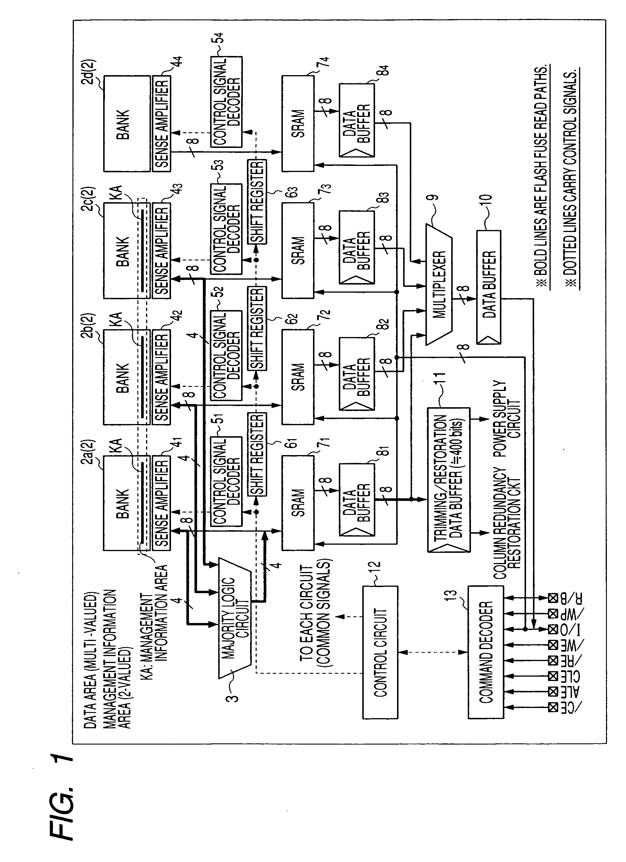
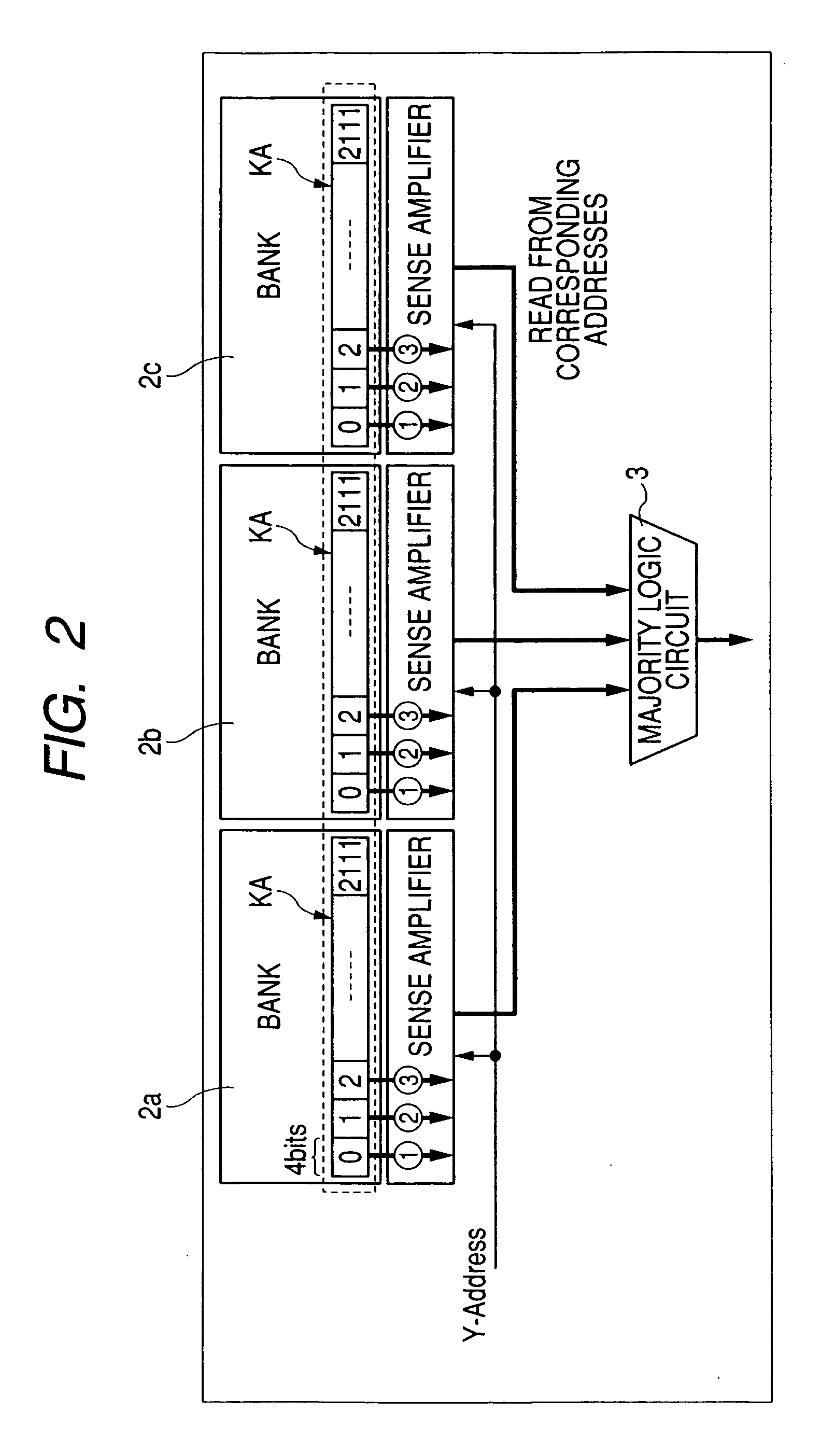
[0027] To explain the present invention in detail, its preferred embodiment is now described, according to the accompanying drawings. In all drawings to explain the preferred embodiment, the same functional components are assigned the same reference numerals and repeated description thereof is omitted.

[0028] In the present embodiment, a flash memory (nonvolatile semiconductor storage device) 1 is the one in which information is stored into a memory cell by setting a plurality of certain levels of threshold voltages and may be either a two-level flash memory to store one bit information in one memory cell or a multilevel flash memory using a multilevel storage technology to store information consisting of two bits or more in one cell.

[0029] As shown in FIG. 1, this flash memory 1 primarily comprises a control block, a memory array 2, and a majority logic circuit 3. The control block is made up of sense amplifiers 41-44, control signal decoders 51-54, shift registers (delay circuits...


PUM


Abstract

The disclosed flash memory is provided with a majority logic circuit 3 and shift registers 61 to 63. Three out of the banks 2a to 2c of the memory respectively include management information areas KAs to store binary management information comprising power supply trimming data and bitline restoration data. During initialization of the flash memory, the majority logic circuit 3 performs error correction on management information bits retrieved from the management information areas KAs and outputs that information to a trimming/restoration data buffer 11, thus providing highly reliable management information very quickly. The shift registers 61 to 63 delay a control signal that is output from a control circuit 12 by a certain period of time before outputting the control signal to sense amplifiers 42 to 44. This delay makes it possible to make the operating currents of the banks 2a to 2d start to flow at different times and to suppress a peak current flowing in the flash memory.

Description

TECHNICAL FIELD [0001] The present invention relates to a nonvolatile semiconductor storage device and, more particularly, to an effective technique for reading management information at a higher speed from a multivalue flash memory. BACKGROUND ART [0002] A flash memory is one type of nonvolatile memory that is electrically programmable and erasable. As is known, the flash memory typically consists of an array of AND-type memory cells in which charging and discharging a floating gate, using a tunnel current, are performed for data writing and erasure. [0003] As the present inventors examined such a flash memory, we have known that the flash memory is furnished with management information comprising power supply trimming data, bitline restoration data, and the like by programming fuses. When the flash memory is initialized upon its power-on or the like, the management information stored in the fuses of the flash memory are read, a fine adjustment of voltage that a power supply circui...

Claims


Application Information

Patent Timeline
IPC IPC(8): G11C16/20G11C16/26
CPCG11C16/26G11C16/20
Inventor HORII, TAKASHIMATSUBARA, KENYOSHIDA, KEIICHI
Owner RENESAS ELECTRONICS CORP
Why Eureka
Try Eureka